
Datasheet


_______________Detailed Description
The MAX195 uses a successive-approximation register
(SAR) to convert an analog input to a 16-bit digital
code, which outputs as a serial data stream. The data
bits can be read either during the conversion, at the
CLK clock rate, or between conversions asynchronous
with CLK at the SCLK rate (up to 5Mbps).
The MAX195 includes a capacitive digital-to-analog
converter (DAC) that provides an inherent track/hold
input. The interface and control logic are designed for
easy connection to most microprocessors (µPs), limiting
the need for external components. In addition to the
SAR and DAC, the MAX195 includes a serial interface, a
sampling comparator used by the SAR, ten calibration
DACs, and control logic for calibration and conversion.
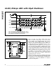
The DAC consists of an array of 16 capacitors with
binary weighted values plus one “dummy LSB” capaci-
tor (Figure 1). During input acquisition in unipolar
mode, the array’s common terminal is connected to
AGND and all free terminals are connected to the input
signal (AIN). After acquisition, the common terminal is
disconnected from AGND and the free terminals are
disconnected from AIN, trapping a charge proportional
to the input voltage on the capacitor array.
The free terminal of the MSB (largest) capacitor is con-
nected to the reference (REF), which pulls the common
terminal (connected to the comparator) positive.
Simultaneously, the free terminals of all other capaci-
tors in the array are connected to AGND, which drives
the comparator input negative. If the analog input is
near V
REF
, connecting the MSB’s free terminal to REF
only pulls the comparator input slightly positive.
However, connecting the remaining capacitor’s free ter-
minals to ground drives the comparator input well
below ground, so the comparator input is negative, the
comparator output is low, and the MSB is set high. If
the analog input is near ground, the comparator output
is high and the MSB is low.
Following this, the next largest capacitor is disconnect-
ed from AGND and connected to REF, and the com-
parator determines the next bit. This continues until all
bits have been determined. For a bipolar input range,
the MSB capacitor is connected to REF rather than AIN
during input acquisition, which results in an input range
of V
REF
to -V
REF
.
MAX195
16-Bit, 85ksps ADC with 10µA Shutdown
_______________________________________________________________________________________ 5
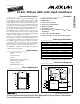
______________________________________________________________Pin Description
PIN NAME FUNCTION
1
BP/UP/SHDN
Bipolar/Unipolar/Shutdown Input. Three-state input selects bipolar or unipolar input range, or shutdown.
0V = shutdown, +5V = unipolar, floating = bipolar.
2 CLK Conversion Clock Input
3 SCLK Serial Clock Input is used to shift data out between conversions. May be asynchronous to CLK.
4 VDDD +5V Digital Power Supply
5 DOUT Serial Data Output, MSB first
6 DGND Digital Ground
7
EOC
End-of-Conversion/Calibration Output—normally low. Rises one clock cycle after the beginning of conversion
or calibration and falls one clock cycle after the end of either. May be used as an output framing signal.
8
CS
Chip-Select Input—active low. Enables the serial interface and the three-state data output (DOUT).
9
CONV
Convert-Start Input—active low. Conversion begins on the falling edge after CONV goes low if the input
signal has been acquired; otherwise, on the falling clock edge after acquisition.
10
RESET
Reset Input. Pulling RESET low places the ADC in an inactive state. Rising edge resets control logic and
begins calibration.
11 VSSD -5V Digital Power Supply
12 REF Reference Input, 0 to 5V
13 AIN Analog Input, 0 to V
REF
unipolar or ±V
REF
bipolar range
14 AGND Analog Ground
15 VSSA -5V Analog Power Supply
16 VDDA +5V Analog Power Supply