
Datasheet


MAX194
Complete source code for the Motorola 68HC16 and
the MAX194 evaluation kit (EV kit) using this mode is
available in the MAX194 EV kit manual.
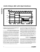
Mode 2 (Asynchronous Data Transfer)
This mode uses a conversion clock (CLK) and a serial
clock (SCLK). The serial data is clocked out between
conversions, which reduces the maximum throughput
for high CLK rates, but may be more convenient for
some applications. Figure 19 is a block diagram with a
QSPI processor (Motorola 68HC16) connected to the
MAX194. Figure 20 shows the associated timing dia-
gram. Figure 21 gives an assembly language listing for
this arrangement.
An OR gate is used to synchronize the “start” signal to
the asynchronous CLK, as described in the
External
Clock
section. As with Mode 1, the QSPI processor must
run CLK during calibration and either count CLK cycles
or, as is done here, monitor EOC to determine when cal-
ibration is complete. Also, EOC is polled by the µP to
determine when a conversion result is available. When
EOC goes low, data is clocked out at the highest QSPI
data rate (4.19Mbps). After the data is transferred, a
new conversion can be initiated whenever desired.
The timing specification for SCLK-to-DOUT valid (t
SD
)
imposes some constraints on the serial interface. At
SCLK rates up to 2.5Mbps, data is clocked out of the
MAX194 by a falling edge of SCLK and may be
clocked into the µP by the next rising edge (CPOL = 0,
CPHA = 0). For data rates greater than 2.5Mbps (or for
lower rates, if desired) it is necessary to clock data out
of the MAX194 on SCLK’s falling edge and to clock it
into the µP on SCLK’s next falling edge (CPOL = 0,
CPHA = 1). Also, your processor hold time must not
exceed t
SD
minimum (20ns). As with CLK in mode 1,
maximum SCLK rates may not be possible with some
interface specifications that are subsets of SPI.
Supplies, Layout, Grounding
and Bypassing
For best system performance, use printed circuit boards
with separate analog and digital ground planes. Wire-
wrap boards are not recommended. The two ground
planes should be tied together at the low-impedance
power-supply source and at the MAX194, as shown in
Figure 22. If the analog and digital supplies come from
the same source, isolate the digital supply from the ana-
log supply with a low-value resistor (10Ω).
14-Bit, 85ksps ADC with 10µA Shutdown
18 ______________________________________________________________________________________
CS
CLK
START
588ns
239ns
CONVERSION TIME
4.19MHz
1.3µs 9.4µs 17µs 5.1µs
4µs
EOC
SCLK
DOUT
B13 B1 B0B11B12 S1 S0
Figure 20. Timing Diagram for Circuit of Figure 19