
Datasheet


Input Acquisition and Settling
Four conversion-clock periods are allocated for acquir-
ing the input signal. At the highest conversion rate, four
clock periods is 2.4µs. If more than three clock cycles
have occurred since the end of the previous conver-
sion, conversion begins on the next falling clock edge
after CONV goes low. Otherwise, bringing CONV low
begins a conversion on the fourth falling clock edge
after the previous conversion. This scheme ensures the
minimum input acquisition time is four clock periods.
Most applications require an input buffer amplifier. If
the input signal is multiplexed, the input channel should
be switched near the beginning of a conversion, rather
than near the end of or after a conversion (Figure 13).
This allows time for the input buffer amplifier to respond
to a large step change in input signal. The input amplifi-
er must have a high enough slew rate to complete the
required output voltage change
before
the beginning of
the acquisition time.
At the beginning of acquisition, the capacitive DAC is
connected to the amplifier output, causing some output
disturbance. Ensure that the sampled voltage has set-
tled to within the required limits before the end of the
acquisition time. If the frequency of interest is low, AIN
can be bypassed with a large enough capacitor to
charge the capacitive DAC with very little change in
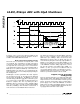
voltage (Figure 14). However, for AC use, AIN must be
driven by a wideband buffer (at least 10MHz), which
must be stable with the DAC’s capacitive load (in paral-
lel with any AIN bypass capacitor used) and also must
settle quickly (Figure 15 or 16).
Digital Noise
Digital noise can easily be coupled to AIN and REF.
The conversion clock (CLK) and other digital signals
that are active during input acquisition contribute noise
to the conversion result. If the noise signal is synchro-
nous to the sampling interval, an effective input offset is
produced. Asynchronous signals produce random
noise on the input, whose high-frequency components
may be aliased into the frequency band of interest.
Minimize noise by presenting a low impedance (at the
frequencies contained in the noise signal) at the inputs.
This requires bypassing AIN to AGND, or buffering the
input with an amplifier that has a small-signal band-
width of several megahertz, or preferably both. AIN has
a bandwidth of about 16MHz.
Offsets resulting from synchronous noise (such as the
conversion clock) are canceled by the MAX194’s cali-
bration scheme. However, because the magnitude of
the offset produced by a synchronous signal depends
on the signal’s shape, recalibration may be appropriate
if the shape or relative timing of the clock or other digi-
tal signals change, as might occur if more than one
clock signal or frequency is used.
Distortion
Avoid degrading dynamic performance by choosing an
amplifier with distortion much less than the MAX194’s
THD (-90dB, or 0.0032%) at frequencies of interest. If
the chosen amplifier has insufficient common-mode
rejection, which results in degraded THD performance,
use the inverting configuration (positive input ground-
ed) to eliminate errors from this source. Low tempera-
ture-coefficient, gain-setting resistors reduce linearity
errors caused by resistance changes due to self-heat-
ing. Also, to reduce linearity errors due to finite amplifier
gain, use an amplifier circuit with sufficient loop gain at
the frequencies of interest (Figures 14, 15, 16).
MAX194
14-Bit, 85ksps ADC with 10µA Shutdown
______________________________________________________________________________________ 15
MAX410
4
7
6
2
3
IN
+5V
-5V
0.1µF 0.01µF
22Ω
510Ω
0.1µF
AIN
Figure 16. ±5V Buffer for AC/DC Use Has ±3.5V Swing