
Datasheet


MAX1719/MAX1720/MAX1721
SOT23, Switched-Capacitor
Voltage Inverters with Shutdown
6 _______________________________________________________________________________________
Charge-Pump Output
The MAX1719/MAX1720/MAX1721 are not voltage reg-
ulators: the charge pumps’ output resistance is
approximately 23Ω at room temperature (with V
IN
=
+5V), and V
OUT
approaches -5V when lightly loaded.
V
OUT
will droop toward GND as load current increases.
The droop of the negative supply (V
DROOP-
) equals the
current draw from OUT (I
OUT
) times the negative con-
verter’s output resistance (R
O
):
V
DROOP-
= I
OUT
x R
O
The negative output voltage will be:
V
OUT
= -(V
IN
- V
DROOP-
)
Efficiency Considerations
The efficiency of the MAX1719/MAX1720/MAX1721 is
dominated by its quiescent supply current (I
Q
) at low
output current and by its output impedance (R
OUT
) at
higher output current; it is given by:
where the output impedance is roughly approximated
by:
The first term is the effective resistance of an ideal
switched-capacitor circuit (Figures 3a and 3b), and
R
SW
is the sum of the charge pump’s internal switch
resistances (typically 8Ω to 9Ω at V
IN
= +5V). The typi-
cal output impedance is more accurately determined
from the Typical Operating Characteristics.
Shutdown Mode
The MAX1719/MAX1720/MAX1721 have a logic-con-
trolled shutdown input. Driving SHDN low places the
MAX1720/MAX1721 in a low-power shutdown mode.
The MAX1719’s shutdown input is inverted from that of
the MAX1720/MAX1721. Driving SHDN high places the
MAX1719 in a low-power shutdown mode. The charge-
pump switching halts, supply current is reduced to
1nA, and OUT is actively pulled to ground through a 4Ω
resistance.
Applications Information
Capacitor Selection
To maintain the lowest output resistance, use capaci-
tors with low ESR (Table 1). The charge-pump output
resistance is a function of C1’s and C2’s ESR.
Therefore, minimizing the charge-pump capacitor’s
ESR minimizes the total output resistance. Table 2
gives suggested capacitor values for minimizing output
resistance or minimizing capacitor size.
R
1
fC1
2R 4ESR ESR
OUT
OSC
SW C1 C2
≅
()
×
++ +
η≅
+
−
×
I
II
IR
V
OUT
OUT Q
OUT OUT
IN
1
S1
IN
S2
S3 S4
C1
C2
V
OUT
= -(V
IN
)
Figure 2. Ideal Voltage Inverter
V+
C1
f
C2 R
L
V
OUT
Figure 3a. Switched-Capacitor Model
R
EQUIV
=
R
EQUIV
V
OUT
R
L
1
V+
f
×
C1
C2
Figure 3b. Equivalent Circuit
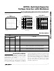
NOTE: ( ) CAPACITORS ARE FOR MAX1720.
*ON/OFF POLARITY OF SHDN IS REVERSED FOR MAX1719.
C1
1
µ
F (10
µ
F)
C2
1
µ
F (10
µ
F)
21
5
ON
OFF
3
R
L
6
4
C3
1
µ
F (10
µ
F)
C1+ C1-
IN
SHDN
OUT
GND
INPUT
1.5V to 5.5V
NEGATIVE
OUTPUT
-1 · V
IN
25mA
MAX1719*
MAX1721
Figure 1. Typical Application Circuit