
Datasheet


MAX17007/MAX17008
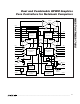
Dual and Combinable QPWM Graphics
Core Controllers for Notebook Computers
12 ______________________________________________________________________________________
Pin Description (continued)
PIN NAME FUNCTION
5 SKIP
Pulse-Skipping Control Input. This four-level input determines the mode of operation under normal
steady-state conditions and dynamic output-voltage transitions:
V
DD
(5V) = Forced-PWM operation
Open (3.3V) = Ultrasonic mode (without forced-PWM during transitions)
REF (2V) = Pulse-skipping mode (with forced-PWM during transitions)
GND = Pulse-skipping mode (without forced-PWM during transitions)
There are no dynamic transitions for SMPS2, so SKIP = 2V and SK IP = GND have the same pulse-
skipping behavior for SMPS2 without any forced-PWM transitions.
In combined mode, the ultrasonic mode is disabled, and the SKIP = OPEN (3.3V) setting is identical
to the SKIP = GND setting.
6 TON1
Frequency-Setting Input for SMPS1. An external resistor between the input power source and TON1
sets the switching period (T
SW1
) of SMPS1:
T
SW1
= C
TON
(R
TON1
+ 6.5k)
where C
TON
= 16.26pF.
TON1 is high impedance in shutdown.
In combined mode, TON1 sets the switching period for both SMPS1 and SMPS2.
7 TON2
Frequency-Setting Input for SMPS2. An external resistor between the input power source and TON2
sets the switching period (T
SW2
) of SMPS2:
T
SW2
= C
TON
(R
TON2
+ 6.5k)
where C
TON
= 16.26pF.
Set TON2 to a switching frequency different from TON1. A 10% to 30% difference in switching
frequency between SMPS1 and SMPS2 is recommended.
TON2 is high impedance in shutdown.
In combined mode, TON2 cannot be left open.
8 REFIN1
External Reference Input for SMPS1. REFIN1 sets the feedback regulation voltage of CSL1. SMPS1
includes an internal window comparator to detect REFIN1 voltage changes that are greater than
±50mV (typ), allowing the controller to blank PGOOD1 and the fault protection, and force the output
transition, if enabled. When REFIN1 is tied to V
CC
, SMPS1 regulates the output to 1.05V.
In combined mode, REFIN1 sets the feedback regulation voltage of the combined output.
9 CSL1
Output-Sense and Negative Current-Sense Input for SMPS1. When using the internal preset 1.05V
feedback divider (REFIN1 = V
CC
), the controller uses CSL1 to sense the output voltage. Connect to
the negative terminal of the current-sense element. Figure 14 describes two different current-sensing
options—using accurate sense resistors or lossless inductor DCR sensing.
10 CSH1
Positive Current-Sense Input for SMPS1. Connect to the positive terminal of the current-sense
element. Figure 14 describes two different current-sensing options—using accurate sense resistors
or lossless inductor DCR sensing.
11 EN1
Enable Control Input for SMPS1. Connect to V
CC
for normal operation. Pull EN1 low to disable
SMPS1. The controller slowly ramps down the output voltage to ground and after the target voltage
reaches 0.1V, the controller forces DL1 low. When both EN1 and EN2 are low, the device enters the
low-power shutdown state.
In combined mode, EN1 controls the combined SMPS output. EN2 is unused and must be grounded.
12 PGOOD1
Open-Drain Power-Good Output for SMPS1. PGOOD1 is low when the SMPS1 voltage is more than 200mV
below or 300mV above the target voltage, during soft-start, and in shutdown. After the SMPS1 soft-start
circuit has terminated, PGOOD1 becomes high impedance 200µs after the output is in regulation. PGOOD1
is blanked (forced high-impedance state) when a dynamic REFIN1 transition is detected.
13 DH1 High-Side Gate-Driver Output for SMPS1. DH1 swings from LX1 to BST1. DH1 is low in shutdown.