
Datasheet


MAX16993 Step-Down Controller with
Dual 2.1MHz Step-Down DC-DC Converters
www.maximintegrated.com
Maxim Integrated
│
22
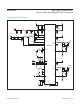
PCB Layout Guidelines
Careful PCB layout is critical to achieve low switching
losses and clean, stable operation. Use a multilayer board
whenever possible for better noise immunity and power
dissipation. Follow these guidelines for good PCB layout:
1) Use a large contiguous copper plane under the device
package. Ensure that all heat-dissipating components
have adequate cooling.
2) Isolate the power components and high-current path
from the sensitive analog circuitry. This is essential to
prevent any noise coupling into the analog signals.
3) Keep the high-current paths short, especially at the
ground terminals. This practice is essential for stable,
jitter-free operation. The high-current path comprising
of input capacitor, high-side FET, inductor, and the
output capacitor should be as short as possible.
4) Keep the power traces and load connections short. This
practice is essential for high efficiency. Use thick copper
PCBs (2oz vs. 1oz) to enhance full-load efficiency.
5) The analog signal lines should be routed away from
the high-frequency planes. This ensures integrity of
sensitive signals feeding back into the device.
6) Use a single ground plane to reduce the chance of
ground-potential differences. With a single ground
plane, enough isolation between analog return signals
and high-power signals must be maintained.