
Datasheet


MAX16836
High-Voltage, 350mA, High-Brightness LED
Driver with PWM Dimming and 5V Regulator
2 _______________________________________________________________________________________
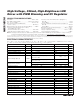
ABSOLUTE MAXIMUM RATINGS
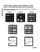
ELECTRICAL CHARACTERISTICS
(V
IN
= V
EN
= +12V, C
V5
= 0.1µF to GND, I
V5
= 0, V
CS-
= 0V, V
DIM
= +4V, connect R
SENSE
= 0.58Ω between CS+ and CS-.
T
A
= -40°C to +125°C, unless otherwise noted. Typical values are at T
A
= +25°C.) (Note 2)
Stresses beyond those listed under “Absolute Maximum Ratings” may cause permanent damage to the device. These are stress ratings only, and functional
operation of the device at these or any other conditions beyond those indicated in the operational sections of the specifications is not implied. Exposure to
absolute maximum rating conditions for extended periods may affect device reliability.
Note 1: Package thermal resistances obtained using the method described in JEDEC specification JESD51-7, using a four-layer
board. For detailed information on package thermal considerations, see www.maxim-ic.com/thermal-tutorial
.
IN to GND ...............................................................-0.3V to +45V
OUT, DIM, and EN to GND..........................-0.3V to (V
IN
+ 0.3V)
CS+, CS-, V5 to GND ...............................................-0.3V to +6V
OUT Short Circuited to GND Duration
(at V
IN
= +16V) .........................................................60 minutes
Maximum Current into Any Pin (except IN and OUT) .........±20mA
Continuous Power Dissipation (T
A
= +70°C)
16-Pin TQFN 5mm x 5mm
(derate 33.3mW/°C above +70°C)............................2666.7mW
8-Pin SO (derate 23.3mW/°C above +70°C).............1860.5mW
Junction-to-Case Thermal Resistance (θ
JC
)(Note 1)
8-Pin SO ...........................................................................7°C/W
16-Pin TQFN.....................................................................2°C/W
Junction-to-Ambient Thermal Resistance (θ
JA
)(Note 1)
8-Pin SO .........................................................................43°C/W
16-Pin TQFN...................................................................30°C/W
Operating Junction Temperature Range...........-40°C to +125°C
Junction Temperature......................................................+150°C
Storage Temperature Range .............................-65°C to +150°C
Lead Temperature (soldering, 10s) .................................+300°C
PARAMETER SYMBOL CONDITIONS MIN TYP MAX UNITS
Supply Voltage Range V
IN
(Note 3) 6.5 40.0 V
Ground Current I
G
I
LOAD
= 350mA 1.28 3 mA
Shutdown Supply Current I
SHDN
V
EN
≤ 0.6V 35 70 µA
Guaranteed Output Current I
OUT
R
SENSE
= 0.55Ω 350 mA
Output Current Accuracy 35mA < I
OUT
< 350mA ±3.5 %
I
OUT
= 350mA (current pulsed),
12V < V
IN
< 40V
0.55 1.2
Dropout Voltage (Note 4) ∆VDO
I
OUT
= 350mA (current pulsed),
6.5V < V
IN
< 12V
0.55 1.5
V
Current rising, V
DIM
rising to 4V 7.8
Output Current Slew Rate
Current falling, V
DIM
falling to 0.6V 7.8
mA/µs
Short-Circuit Current V
IN
= 12V, V
CS+
= 0V 400 500 650 mA
LOGIC INPUT
EN Input Current I
EN
-2.5 -1.0 -0.2 µA
EN Input Voltage High V
IH
2.8 V
EN Input Voltage Low V
IL
0.6 V
Turn-On Time t
ON
V
EN
rising edge to 90% of OUT 110 350 µs
CURRENT SENSE
Regulated R
SENSE
Voltage V
SENSE
V
SENSE
= V
CS+
- V
CS-
193 200 207 mV
CS- Voltage Range -0.3 +4.1 V
Input Current (CS+) V
CS+
= 220mV 2.7 7.0 µA
Input Current (CS-) V
CS+
= 220mV -50 17.2 µA
DIM Input Current -2.5 -1.0 -0.2 µA
DIM Input Voltage High V
IH
4V
DIM Input Voltage Low V
IL
0.6 V
Turn-On Time t
ON
After V
DIM
rising to 4V (Note 5) 110 µs
Turn-Off Time t
OFF
After V
DIM
falling to 0.6V (Note 5) 70 µs