
Datasheet

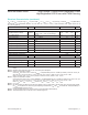


PIN
NAME FUNCTION
TDFN SO
1 6 DIM
Pulsed Dimming Input. Drive DIM low to turn off output current (LED current). Drive DIM
high to turn on the output current (LED current). DIM is pulled high to V
IN
when left
unconnected
— 7 EN
Enable Input. Drive EN high to enable the output. For the TDFN package, this input is not
accessible and always high
2 8 OUT Current-Regulated Output
3 1 IN Positive Input Supply. Bypass IN with a 0.1µF (min) capacitor to GND
4 2 CS+
LED Current-Sense Amplifier Positive Input. For the SO package version, connect the
current-sense resistor between this pin and CS-; for the TDFN version, connect it between
this pin and ground.
— 3 CS- LED Current-Sense Amplifier Negative Input. Connect to ground
5 4 V5 +5V Regulated Output. Connect a 0.1µF (min) capacitor from V5 to GND
6 5 GND Ground
— — EP
Exposed Pad. Connect to a large ground plane for effective power dissipation. Do not use as
the only ground connection.
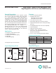
BANDGAP
AND 5V
REGULATOR
THERMAL
SHUTDOWN
GND
V5
1.2V
DIM IN
P
OUT
CS+
0.8A
MAX16815
MAX16828
IREG
DIFF
AMP
www.maximintegrated.com
Maxim Integrated
│
6
MAX16815/MAX16828 High-Voltage, 100mA/200mA Adjustable Linear
High-Brightness LED Drivers with PWM Dimming
DFN Functional Diagram
Pin Description