
Datasheet


MAX1652–MAX1655
High-Efficiency, PWM, Step-Down
DC-DC Controllers in 16-Pin QSOP
10 ______________________________________________________________________________________
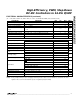
Standard Application Circuits
It’s easy to adapt the basic MAX1653 single-output 3.3V
buck converter (Figure 1) to meet a wide range of appli-
cations with inputs up to 30V (limited by choice of exter-
nal MOSFET). Simply substitute the appropriate
components from Table 1 (candidate suppliers are pro-
vided in Table 2). These circuits represent a good set of
trade-offs among cost, size, and efficiency while staying
within the worst-case specification limits for stress-relat-
ed parameters such as capacitor ripple current.
Don’t change the frequency of these circuits without
first recalculating component values (particularly induc-
tance value at maximum battery voltage).
For a discussion of dual-output circuits using the
MAX1652 and MAX1654, see Figure 9 and the
Secondary Feedback-Regulation Loop
section.
Detailed Description
The MAX1652 family are BiCMOS, switch-mode power-
supply controllers designed primarily for buck-topology
regulators in battery-powered applications where high
efficiency and low quiescent supply current are critical.
The parts also work well in other topologies such as
boost, inverting, and Cuk due to the flexibility of their
floating high-speed gate driver. Light-load efficiency is
enhanced by automatic idle-mode operation—a vari-
able-frequency pulse-skipping mode that reduces
losses due to MOSFET gate charge. The step-down
power-switching circuit consists of two N-channel
MOSFETs, a rectifier, and an LC output filter. The out-
put voltage is the average of the AC voltage at the
switching node, which is adjusted and regulated by
changing the duty cycle of the MOSFET switches. The
gate-drive signal to the N-channel high-side MOSFET
must exceed the battery voltage and is provided by a
flying capacitor boost circuit that uses a 100nF capaci-
tor connected to BST.
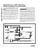
MAX1653
CSL
CSH
VL
SYNC
FB
V+
10 11
57
14
Q1
Q2
16
15
13
D2
CMPSH-3
J1
150kHz/300kHz
JUMPER
NOTE: KEEP CURRENT-SENSE
LINES SHORT AND CLOSE
TOGETHER. SEE FIGURE 8.
D1
12
8
9
REF
3
GND
4
+5V AT
5mA
+3.3V
OUTPUT
GND
OUT
BST
DH
LX
DL
2
1
LOW-NOISE
CONTROL
PGND
SKIP
SS
6
ON/OFF
CONTROL
SHDN
INPUT
REF OUTPUT
+2.5V AT 100µA
C5
0.33µF
C4
4.7µF
C7
0.1µF
C6
0.01µF
(OPTIONAL)
C1
C2
C3
0.1µF
R1
L1
Figure 1. Standard 3.3V Application Circuit (see Table 1 for Component Values)