
Datasheet


MAX16016/MAX16020/MAX16021
Low-Power µP Supervisory Circuits with
Battery-Backup Circuit and Chip-Enable Gating
_______________________________________________________________________________________ 9
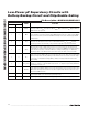
Pin Description—MAX16016
PIN NAME FUNCTION
1V
CC
Supply Voltage Input. Bypass V
CC
to GND with a 0.1µF capacitor.
2 BATT
Backup Battery Input. If V
CC
falls below its reset threshold, and if V
BATT
> V
CC
, OUT connects to
BATT. If V
CC
rises above 1.01 x V
BATT
, OUT connects to V
CC
. Bypass BATT
to GND with a 0.1µF
capacitor.
3 MR
Active-Low Manual Reset Input. RESET asserts when MR is pulled low. RESET remains low for the
duration of reset timeout period after MR transitions from low to high. Connect MR to V
CC
or leave
unconnected if not used. MR is internally connected to V
CC
through a 30kΩ pullup resistor.
4 PFI
Power-Fail Comparator Input. Connect PFI to a resistive divider to set the desired PFI threshold. The
PFI input is referenced to an internal V
PFT
threshold. A V
PFT-HYS
internal hysteresis provides noise
immunity. The power-fail comparator is powered from OUT.
5 WDI
Watchdog Timer Input. If WDI remains high or low for longer than the watchdog timeout period (t
WD
),
the internal watchdog timer runs out and a reset pulse is triggered for the reset timeout period. The
internal watchdog clears when reset asserts or whenever WDI sees a rising or falling edge. To
disable the watchdog feature, leave WDI unconnected or three-state the driver connected to WDI.
6 BATTON Acti ve- H i g h Batter y- O n Outp ut. BATTON g oes hi g h w hen i n b atter y- b ackup m od e.
7 PFO
Active-Low Power-Fail Comparator Output. PFO goes low when V
PFI
falls below the internal V
PFT
threshold and goes high when V
PFI
rises above V
PFT
+ V
PFT-HYS
hysteresis.
8 GND Ground
9 RESET
Acti ve- Low Reset Outp ut. RESET asser ts w hen V
C C
fal l s b el ow the r eset thr eshol d or M R i s p ul l ed l ow .
RESET r em ai ns l ow for the d ur ati on of the r eset ti m eout p er i od after V
C C
r i ses ab ove the r eset thr eshol d
and M R g oes hi g h. RESET al so asser ts l ow w hen the i nter nal w atchd og ti m er r uns out.
10 OUT
Switched Output. OUT is connected to V
CC
when the reset output is not asserted or when V
CC
is
greater than V
BATT
. OUT connects to BATT when RESET is asserted and V
BATT
is greater than V
CC
.
Bypass OUT
to GND with a 0.1µF (min) capacitor.