
Datasheet


Note 1: V
DD
= +5V, V
REFIN
= +2.5V, V
SS
= 0V. Performance at ±5% power-supply tolerance is guaranteed by Power-Supply
Rejection test.
Note 2: Guaranteed by design, not production tested.
Note 3: All input control signals are specified with t
r
= t
f
= 20ns (10% to 90% of +5V) and timed from a +1.6V voltage level. Output
signals are timed from V
OH
and V
OL
.
Note 4: t
DV
is the time required for an output to cross +0.8V or +2.4V measured with load circuit of Figure 1.
Note 5: t
TR
is the time required for the data lines to change 0.5V, measured with load circuits of Figure 2.
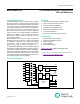
Figure 1. Load Circuits for Data-Access Timing
Figure 2. Load Circuits for Three-State Output Timing
PARAMETER SYMBOL CONDITIONS MIN TYP MAX UNITS
BUSY High to WR Delay (to update
conguration register) (Notes 2, 3)
t
BWD
50 ns
CLK to WR Delay (Acquisition Time)
(Note 2)
t
ACQ
800 ns
BUSY High to RD Delay (Notes 2, 3) t
BRD
50 ns
Address-Setup Time t
AS
120 ns
Address-Hold Time t
AH
0 ns
RD to Data Valid (Note 4) t
DV
MAX15_C/E 100 ns
RD to Data Three-State Output (Note 5) t
TR
MAX15_C/E 80 ns
CLK to BUSY Delay (Note 2) t
CB
100 300 ns
CLK Frequency 0.5 5.0 MHz
DN
3kΩ
3kΩ
DGND
HIGH-Z TO V
OH
100pF
DN
+5V
HIGH-Z TO V
OL
100pF
DGND
DN
3kΩ
3kΩ
V
OH
TO HIGH-Z
10pF
DN
+5V
V
OL
TO HIGH-Z
10pF
MAX155/MAX156 8-/4-Channel ADCs with Simultaneous
T/Hs and Reference
www.maximintegrated.com
Maxim Integrated
│
5
TIMING CHARACTERISTICS (Note 3, Figures 1-7) (continued)
(V
DD
= +5V, V
REFIN
= +2.5V. External Reference, V
AGND
= V
DGND
= 0V, V
SS
= 0V or -5V, T
A
= T
MIN
to T
MAX
, unless otherwise noted.)