
Datasheet


General Description
The MAX1510/MAX17510 DDR linear regulators source
and sink up to 3A peak (typ) using internal n-channel
MOSFETs. These linear regulators deliver an accurate
0.5V to 1.5V output from a low-voltage power input (V
IN
= 1.1V to 3.6V). The MAX1510/MAX17510 use a sepa-
rate 3.3V bias supply to power the control circuitry and
drive the internal n-channel MOSFETs.
The MAX1510/MAX17510 provide current and thermal
limits to prevent damage to the linear regulator.
Additionally, the MAX1510/MAX17510 generate a
power-good (PGOOD) signal to indicate that the output
is in regulation. During startup, PGOOD remains low
until the output is in regulation for 2ms (typ). The internal
soft-start limits the input surge current.
The MAX1510/MAX17510 power the active-DDR termi-
nation bus that requires a tracking input reference. The
MAX1510/MAX17510 can also be used in low-power
chipsets and graphics processor cores that require
dynamically adjustable output voltages. The
MAX1510/MAX17510 are available in a 10-pin, 3mm x
3mm thin DFN package.
Applications
Notebook/Desktop Computers
DDR Memory Termination
Active Termination Buses
Graphics Processor Core Supplies
Chipset/RAM Supplies as Low as 0.5V
Features
o Internal Power MOSFETs with Current Limit (3A typ)
o Fast Load-Transient Response
o External Reference Input with Reference
Output Buffer
o 1.1V to 3.6V Power Input
o ±15mV (max) Load-Regulation Error
o Thermal-Fault Protection
o Shutdown Input
o Power-Good Window Comparator with 2ms
(typ) Delay
o Small, Low-Profile 10-Pin, 3mm x 3mm TDFN
Package
o Ceramic or Polymer Output Capacitors
MAX1510/MAX17510
Low-Voltage DDR Linear Regulators
________________________________________________________________
Maxim Integrated Products
1
Ordering Information
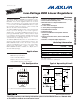
OUT
IN
OUTS
AGND
PGND
V
OUT
= V
TT
V
IN
(1.1V TO 3.6V)
V
BIAS
(2.7V TO 3.6V)
V
DDQ
(2.5V OR 1.8V)
V
REFOUT
= V
TTR
REFOUT
MAX1510
MAX17510
V
CC
PGOOD
SHDN
REFIN
Typical Operating Circuit
19-3279; Rev 5; 3/11
For pricing, delivery, and ordering information, please contact Maxim Direct at 1-888-629-4642,
or visit Maxim’s website at www.maxim-ic.com.
EVALUATION KIT
AVAILABLE
PART TEMP RANGE
PIN-
PACKAGE
TOP
MARK
MAX1510ETB -40°C to +85°C 10 TDFN-EP* ARD
MAX1510ETB+ -40°C to +85°C 10 TDFN-EP* ABD
MAX1510ATB/V+ -40°C to +85°C 10 TDFN-EP* AWD
MAX17510ATB+ - 40° C to + 125° C 10 TDFN-EP* AWQ
MAX17510ATB/V+ - 40° C to + 125° C 10 TDFN-EP* AWQ
SHDN
OUTSPGOOD
OUT
PGND
AGND
REFIN
V
CC
TDFN
3mm x 3mm
TOP VIEW
51234
INREFOUT
MAX1510
MAX17510
A "+" SIGN WILL REPLACE THE FIRST PIN INDICATOR ON LEAD-FREE PACKAGES.
+
610987
Pin Configuration
+
Denotes a lead(Pb)-free and RoHS-compliant package.
*
EP = Exposed pad.
/V denotes an automotive qualified part.