
Datasheet


+2.7V to +5.25V, Low-Power, 8-Channel,
Serial 10-Bit ADCs
MAX148/MAX149
13
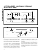
Figure 9. Internal Clock Mode Timing
Internal Clock
In internal clock mode, the MAX148/MAX149 generate
their own conversion clocks internally. This frees the FP
from the burden of running the SAR conversion clock
and allows the conversion results to be read back at
the processor’s convenience, at any clock rate from 0
to 2MHz. SSTRB goes low at the start of the conversion
and then goes high when the conversion is complete.
SSTRB is low for a maximum of 7.5Fs (SHDN = uncon-
nected), during which time SCLK should remain low for
best noise performance.
An internal register stores data when the conversion
is in progress. SCLK clocks the data out of this regis-
ter at any time after the conversion is complete. After
SSTRB goes high, the next falling clock edge produces
the MSB of the conversion at DOUT, followed by the
remaining bits in MSB-first format (Figure 9). CS does
not need to be held low once a conversion is started.
Pulling CS high prevents data from being clocked into
the MAX148/MAX149 and three-states DOUT, but it
does not adversely affect an internal clock mode con-
version already in progress. When internal clock mode
is selected, SSTRB does not go into a high-impedance
state when CS goes high.
Figure 10 shows the SSTRB timing in internal clock
mode. In this mode, data can be shifted in and out of
the MAX148/MAX149 at clock rates exceeding 2.0MHz if
the minimum acquisition time (t
ACQ
) is kept above 1.5Fs.
Data Framing
The falling edge of CS does not start a conversion. The
first logic high clocked into DIN is interpreted as a start
bit and defines the first bit of the control byte. A conver-
sion starts on SCLK’s falling edge, after the eighth bit of
Figure 10. Internal Clock Mode SSTRB Detailed Timing
1
SEL2 SEL1 SEL0 PD0PD1
SGL/
DIF
UNI/
BIP
2 3 4 5 6 7 8 9 10
B9
MSB
B8 B7
B0
LSB
S1 S0
11 12 18 19 20 21 22 23 24
SCLK
DIN
START
SSTRB
1.5Fs 7.5Fs MAX
DOUT
AD STATE
IDLE
IDLE
ACQUISITION CONVERSION
t
CONV
FILLED WITH
ZEROS
CS
(f
SCLK
= 2MHz)(SHDN = UNCONNECTED)
SSTRB
SCLK
NOTE: FOR BEST NOISE PERFORMANCE, KEEP SCLK LOW DURING CONVERSION.
DOUT
PD0 CLOCK IN
t
SSTRB
t
CONV
t
CSH
t
SCK
t
CSS
t
D0
CS