
Datasheet


MAX146/MAX147
+2.7V, Low-Power, 8-Channel,
Serial 12-Bit ADCs
8 _______________________________________________________________________________________
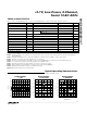
NAME FUNCTION
1–8 CH0–CH7 Sampling Analog Inputs
PIN
9 COM
Ground reference for analog inputs. COM sets zero-code voltage in single-ended mode. Must be
stable to ±0.5LSB.
10
SHDN
Three-Level Shutdown Input. Pulling SHDN low shuts the MAX146/MAX147 down; otherwise, they are
fully operational. Pulling SHDN high puts the reference-buffer amplifier in internal compensation mode.
Letting SHDN float puts the reference-buffer amplifier in external compensation mode.
15 DOUT
Serial Data Output. Data is clocked out at SCLK’s falling edge. High impedance when CS is high.
14 DGND Digital Ground
13 AGND Analog Ground
11 VREF
Reference-Buffer Output/ADC Reference Input. Reference voltage for analog-to-digital conversion.
In internal reference mode (MAX146 only), the reference buffer provides a 2.500V nominal output,
externally adjustable at REFADJ. In external reference mode, disable the internal buffer by pulling
REFADJ to V
DD
.
19 SCLK
Serial Clock Input. Clocks data in and out of serial interface. In external clock mode, SCLK also sets
the conversion speed. (Duty cycle must be 40% to 60%.)
18
CS
Active-Low Chip Select. Data will not be clocked into DIN unless CS is low. When CS is high, DOUT is
high impedance.
17 DIN Serial Data Input. Data is clocked in at SCLK’s rising edge.
16 SSTRB
Serial Strobe Output. In internal clock mode, SSTRB goes low when the MAX146/MAX147 begin the
A/D conversion, and goes high when the conversion is finished. In external clock mode, SSTRB pulses
high for one clock period before the MSB decision. High impedance when CS is high (external clock
mode).
______________________________________________________________Pin Description
V
DD
6kΩ
DGND
DOUT
C
LOAD
50pF
C
LOAD
50pF
DGND
6kΩ
DOUT
a) High-Z to V
OH
and V
OL
to V
OH
b) High-Z to V
OL
and V
OH
to V
OL
V
DD
6kΩ
DGND
DOUT
C
LOAD
50pF
C
LOAD
50pF
DGND
6kΩ
DOUT
a) V
OH
to High-Z b) V
OL
to High-Z
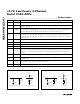
Figure 1. Load Circuits for Enable Time Figure 2. Load Circuits for Disable Time
12 REFADJ Input to the Reference-Buffer Amplifier. To disable the reference-buffer amplifier, tie REFADJ to V
DD
.
20 V
DD
Positive Supply Voltage