
Datasheet


MAX146/MAX147
+2.7V, Low-Power, 8-Channel,
Serial 12-Bit ADCs
_______________________________________________________________________________________ 5
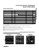
Figure 1
Typical Operating Characteristics
(V
DD
= 3.0V, VREF = 2.5V, f
SCLK
= 2.0MHz, C
LOAD
= 20pF, T
A
= +25°C, unless otherwise noted.)
0.5
0 1024 2048 3072 4096
INTEGRAL NONLINEARITY
vs. CODE
0.3
-0.3
-0.5
-0.1
0.1
0.4
0.2
-0.4
-0.2
0
MAX146/47-01
CODE
INL (LSB)
0.50
0
2.25 2.75 4.25
INTEGRAL NONLINEARITY
vs. SUPPLY VOLTAGE
0.45
0.40
0.35
0.30
0.25
0.20
0.15
0.10
0.05
V
DD
(V)
INL (LSB)
3.75 5.253.25 4.75
MAX146/47-02
MAX146
MAX147
0
0.10
0.20
0.30
0.40
0.50
0.05
0.15
0.25
0.35
0.45
-60 -20 20 60 100 140
INTEGRAL NONLINEARITY
vs. TEMPERATURE
TEMPERATURE
(°C)
INL (LSB)
MAX146/47-03
MAX147
MAX146
V
DD
= 2.7V
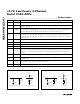
TIMING CHARACTERISTICS
(V
DD
= +2.7V to +3.6V (MAX146); V
DD
= +2.7V to +5.25V (MAX147); T
A
= T
MIN
to T
MAX
; unless otherwise noted.)
Note 1: Tested at V
DD
= 2.7V; COM = 0; unipolar single-ended input mode.
Note 2: Relative accuracy is the deviation of the analog value at any code from its theoretical value after the full-scale range has
been calibrated.
Note 3: MAX146—internal reference, offset nulled; MAX147—external reference (VREF = +2.5V), offset nulled.
Note 4: Ground “on” channel; sine wave applied to all “off” channels.
Note 5: Conversion time defined as the number of clock cycles multiplied by the clock period; clock has 50% duty cycle.
Note 6: The common-mode range for the analog inputs is from AGND to V
DD
.
Note 7: External load should not change during conversion for specified accuracy.
Note 8: ADC performance is limited by the converter’s noise floor, typically 300µVp-p.
Note 9: Guaranteed by design. Not subject to production testing.
Note
10:
Measured as
|
V
FS
(2.7V) - V
FS
(V
DD, MAX
)
|
.
Internal clock mode only (Note 9)
External clock mode only, Figure 2
External clock mode only, Figure 1
DIN to SCLK Setup
Figure 1
Figure 2
Figure 1
MAX14_ _C/E
CONDITIONS
MAX14_ _M
ns
20 240
Figure 1
ns
t
CSH
ns240t
STR
CS Rise to SSTRB Output Disable
ns240t
SDV
CS Fall to SSTRB Output Enable
240t
SSTRB
SCLK Fall to SSTRB ns
200t
CL
SCLK Pulse Width Low
ns200SCLK Pulse Width High
ns0
CS to SCLK Rise Hold
ns100t
CSS
CS to SCLK Rise Setup
ns240t
TR
CS Rise to Output Disable
ns240t
DV
CS Fall to Output Enable
t
CH
20 200
t
DO
SCLK Fall to Output Data Valid
ns0t
DH
DIN to SCLK Hold
ns
µs1.5t
ACQ
Acquisition Time
0t
SCK
SSTRB Rise to SCLK Rise
ns100t
DS
UNITSMIN TYP MAXSYMBOLPARAMETER