
Datasheet


MAX1471
CPU Recovery Timer (t
CPU
)
The second timer, t
CPU
(see Figure 12), is used to delay
the power-up of the MAX1471, thereby providing extra
power savings and giving a CPU the time required to
complete its own power-on sequence. The CPU is sig-
naled to begin powering up when the DIO line is pulled
low by the MAX1471 at the end of t
OFF
. t
CPU
then begins
counting down, while DIO is held low by the MAX1471.
At the end of t
CPU
, the t
RF
counter begins.
t
CPU
is an 8-bit timer, configured through register 0x6.
The possible t
CPU
settings are summarized in Table 11.
The data written to the t
CPU
register (0x6) is multiplied
by 120µs to give the total t
CPU
time. On power-up, the
CPU timer register is set to zero and must be written
before using DRX mode.
RF Settle Timer (t
RF
)
The third timer, t
RF
(see Figure 12), is used to allow the
RF sections of the MAX1471 to power up and stabilize
before ASK or FSK data is received. t
RF
begins count-
ing once t
CPU
has expired. At the beginning of t
RF
, the
modules selected in the power control register (register
0x0) are powered up with the exception of the peak
detectors and have the t
RF
period to settle.
315MHz/434MHz Low-Power, 3V/5V
ASK/FSK Superheterodyne Receiver
20 ______________________________________________________________________________________
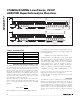
Table 5. Register Configuration
ADDRESS DATA
A3 A2 A1 A0 D7 D6 D5 D4 D3 D2 D1 D0
POWER CONFIGURATION (0x0)
0 0 0 0 LNA_EN AGC_EN
MIXER_
EN
FSKBB_
EN
FSKPD_
EN
ASKBB_
EN
ASKPD_
EN
SLEEP
CONFIGURATION (0x1)
0 0 0 1 X
GAIN
SET*
FSKCALL
SB
FSK_
DOUT
ASK_
DOUT
TOFF_
PS1
TOFF_
PS0
DRX_
MODE
CONTROL (0x2)
0 0 1 0 X
AGC
LOCK
XX
FSKTRK_
EN
ASKTRK_
EN
P OL_
C AL_E N
FSK_CAL
_EN
OSCILLATOR FREQUENCY (0x3)
0 0 1 1 d7d6d5d4d3d2d1d0
OFF TIMER (upper byte) (0x4)
0 1 0 0 t15 t14 t13 t12 t11 t10 t9 t8
OFF TIMER (lower byte) (0x5)
0 1 0 1 t7t6t5t4t3t2t1t0
CPU RECOVERY TIMER (0x6)
0 1 1 0 t7t6t5t4t3t2t1t0
RF SETTLE TIMER (upper byte) (0x7)
0 1 1 1 t15 t14 t13 t12 t11 t10 t9 t8
RF SETTLE TIMER (lower byte) (0x8)
1 0 0 0 t7t6t5t4t3t2t1t0
STATUS REGISTER (read only) (0x9)
1 0 0 1
LOCK
DET
AGCST
CLK
ALIVE
XXX
P OL_C AL
_D O N E
FSK_CAL
_DONE
AGC DWELL TIMER (0xA)
1 0 1 0 X X X dt4 dt3* dt2* dt1 dt0*
*
Power-up state = 1. All other bits, power-up state = 0.