
Datasheet


Calibrate the polling timer by setting POL_CAL_EN = 1
in the configuration register (register 0x1). Upon com-
pletion, the POL_CAL_DONE bit in the status register
(register 0x8) is 1, and the POL_CAL_EN bit is reset to
zero. If using the MAX1471 in continuous receive
mode, polling timer calibration is not needed.
FSK receiver calibration is a two-step process. Set
FSKCALLSB = 1 (register 0x1) or to reduce the calibra-
tion time, accuracy can be sacrificed by setting the
FSKCALLSB = 0. Next, initiate FSK receiver calibration,
set FSK_CAL_EN = 1. Upon completion, the
FSK_CAL_DONE bit in the status register (register 0x8)
is one, and the FSK_CAL_EN bit is reset to zero.
When in continuous receive mode and receiving FSK
data, recalibrate the FSK receiver after a significant
change in temperature or supply voltage. When in dis-
continuous receive mode, the polling timer and FSK
receiver (if enabled) are automatically calibrated during
every wake-up cycle.
Off Timer (t
OFF
)
The first timer, t
OFF
(see Figure 12), is a 16-bit timer
that is configured using: register 0x4 for the upper byte,
register 0x5 for the lower byte, and bits PRESCALE1
and PRESCALE0 in the configuration register (register
0x1). Table 10 summarizes the configuration of the t
OFF
timer. The PRESCALE1 and PRESCALE2 bits set the
size of the shortest time possible (t
OFF
time base). The
data written to the t
OFF
registers (0x4 and 0x5) is multi-
plied by the time base to give the total t
OFF
time. On
power-up, the off timer registers are set to zero and
must be written before using DRX mode.
During t
OFF
, the MAX1471 is operating with very low
supply current (5.0µA typ), where all of its modules are
turned off, except for the t
OFF
timer itself. Upon com-
pletion of the t
OFF
time, the MAX1471 signals the user
by asserting DIO low.
MAX1471
315MHz/434MHz Low-Power, 3V/5V
ASK/FSK Superheterodyne Receiver
______________________________________________________________________________________ 19
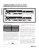
Table 4. Register Summary
REGISTER
A[3:0]
REGISTER NAME DESCRIPTION
0x0 Power configuration
Enables/disables the LNA, AGC, mixer, baseband, peak detectors, and sleep mode
(see Table 6).
0x1 Configuration
Sets options for the device such as output enables, off-timer prescale, and
discontinuous receive mode (see Table 7).
0x2 Control
Controls AGC lock, peak-detector tracking, as well as polling timer and FSK
calibration (see Table 8).
0x3 Oscillator frequency
Sets the internal clock frequency divisor. This register must be set to the integer
result of f
XTAL
/100kHz (see the Oscillator Frequency Register section).
0x4
Off timer—t
OFF
(upper byte)
0x5
Off timer—t
OFF
(lower byte)
Sets the duration that the MAX1471 remains in low-power mode when DRX is active
(see Table 10).
0x6 CPU recovery timer—t
CPU
Increases maximum time the MAX1471 stays in lower power mode while CPU wakes
up when DRX is active (see Table 11).
0x7
RF settle timer—t
RF
(upper byte)
0x8
RF settle timer—t
RF
(lower byte)
During the time set by the settle timer, the MAX1471 is powered on with the peak
detectors and the data outputs disabled to allow time for the RF section to settle.
DIO must be driven low at any time during t
LOW
= t
CPU
+ t
RF
or the timer sequence
restarts (see Table 12).
0x9 Status register (read only)
Provides status for PLL lock, AGC state, crystal operation, polling timer, and FSK
calibration (see Table 9).
0xA AGC dwell timer Controls the dwell (release) time of the AGC.