
Datasheet


MAX1426
10-Bit, 10Msps ADC
_______________________________________________________________________________________ 3
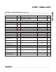
ELECTRICAL CHARACTERISTICS (continued)
(V
AV
DD
= V
CMLP
= +5V, V
DV
DD
= +3.3V, V
CMLN
= V
AGND
= V
DGND
= 0V, internal reference, digital output loading 35pF, f
CLK
=
10MHz (50% duty cycle), T
A
= T
MIN
to T
MAX
, unless otherwise noted. Typical values are at T
A
= +25°C.)
f = 2MHz
CONDITIONS
Bits
9.3 9.7
ENOBEffective Number of Bits
UNITSMIN TYP MAXSYMBOL PARAMETER
f1 = 1.98MHz, f2 = 2.00MHz
(-7dB FS, each tone) (Note 5)
dBc
-70
IMDIntermodulation Distortion
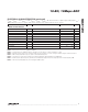
(Note 7)
(Note 7)
V
INP
- V
INN
CML (Note 6)
Either input to ground
Either input to ground
MHz150LSBWLarge-Signal Bandwidth
MHz400SSBWSmall-Signal Bandwidth
V±2DRDifferential Input Range
V
2.25
±10%
V
CMVR
Input Common-Mode Voltage
Range
pF
8
C
IN
Input Capacitance
kΩ
3.5
R
IN
Input Resistance
REFP, CML, REFN
REFP, CML, REFN
V
REFP
- V
REFN
REFIN
REFIN (Note 8)
V
1.25
±10%
REFN Input Range
V
2.25
±10%
CML Input Range
V
3.25
±10%
REFP Input Range
pF
15
C
IN
Input Capacitance
µA
-325 +325
I
IN
Input Current
V
2.0
Differential Reference
pF
10
C
IN
Input Capacitance
kΩ
6.5
R
IN
Input Resistance
V
REFP
- V
REFN,
T
A
= +25°C V
1.9 2.0 2.1
Differential Reference
V
1.25
V
REFN
Negative Reference Input
Voltage
V
2.25
V
CML
Common-Mode Reference
Voltage
V
3.25
V
REFP
Positive Reference Voltage
ppm/°C±50
Differential Reference
Temperature Coefficient
REFERENCE OUTPUTS (REFP, CML, REFN; external +2.5V reference)
REFERENCE (V
REFIN
= 0; REFP, REFN, CML applied externally)
ANALOG INPUT (INP, INN, CML)