
Datasheet


Set CLK = 0 if the external clock frequency is 1MHz
with CLKDIV = 0 or 2MHz with CLKDIV = 1.
FS1, FS0: (Default = 0, 1) Filter-Selection Bits. These bits,
in addition to the CLK bit, determine the output data rate
and the digital filter cutoff frequency. See Table 13 for
FS1 and FS0 settings. Recalibrate when the filter charac-
teristics are changed.
Data Register
The data register is a 16-bit read-only register. Figure 9
shows how to read conversion results using the
data register.
The data from the data register is read through DOUT.
DOUT changes on the falling edge of SCLK and is valid
on the rising edge of SCLK. The data-register format is
16-bit straight binary for unipolar mode with zero scale
equal to 0x0000, and offset binary for bipolar mode
with zero scale equal to 0x1000.
Test Register
This register is reserved for factory testing of the
device. For proper operation of the MAX1415/
MAX1416, do not change this register from its default
power-on reset values.
Offset and Gain-Calibration Registers
The MAX1415/MAX1416 contain one offset register and
one gain register for each input channel. Each register
is 24 bits wide and can be written and read. The offset
registers store the calibration coefficients resulting from
a zero-scale calibration, and the gain registers store
the calibration coefficients resulting from a full-scale
calibration. The data stored in these registers are 24-bit
straight binary values representing the offset or gain
errors associated with the selected channel. A 24-bit
read or write operation can be performed on the cali-
bration registers for any selected channel. During a
write operation, 24 bits of data must be written to the
register, or no data is transferred.
MAX1415/MAX1416
16-Bit, Low-Power, 2-Channel,
Sigma-Delta ADCs
______________________________________________________________________________________ 27
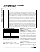
Table 13. Output Data Rate and Notch Frequency vs. Filter Select and CLKIN Frequency
CLKIN FREQUENCY
f
CLKIN
(MHz)*
CLK FS1 FS0
OUTPUT DATA RATE
(FIRST NOTCH) (Hz)
-3dB FILTER CUTOFF**
(Hz)
1 0 0 0 20 5.24
1 0 0 1 25 6.55
1 0 1 0 100 26.2
1 0 1 1 200 52.4
2.4576 1 0 0 50 13.1
2.4576 1 0 1 60 15.7
2.4576 1 1 0 250 65.5
2.4576 1 1 1 500 131
*These values are given for CLKDIV = 0. External-clock frequency, f
CLKIN
, equals two times the values in this column if CLKDIV = 1.
**The filter -3dB filter cutoff frequency = 0.262 x filter first notch frequency.
Table 12. Clock Register
(MSB) (LSB)
FUNCTION RESERVED
INTERNAL
CLOCK ENABLE
CLOCK
DISABLE
CLOCK
DIVIDER
CLOCK
SELECT
FILTER SELECT
Name MXID ZERO INTCLK CLKDIS CLKDIV CLK FS1 FS0
Defaults 1 0 0 0 0 1 0 1