
Datasheet


MAX1407/MAX1408/MAX1409/MAX1414
Low-Power, 16-Bit Multichannel DAS with
Internal Reference,10-Bit DACs, and RTC
______________________________________________________________________________________ 29
WU2: Wake-Up2 status bit. When WU2 is pulled low,
WU2 is set to a logic 1. Reading the Status register
clears WU2, unless WU2 is still low. When WU2 is
pulled low when the device is awake (not in Sleep
mode), WU2 is cleared.
WU1: Wake-Up1 status bit. When WU1 is pulled low,
WU1 is set to a logic 1. Reading the Status register
clears WU1, unless WU1 is still low. When WU1 is
pulled low when the device is awake (not in Sleep
mode), WU1 is cleared.
RST: Reset status bit. When AV
DD
drops below the
RESET Voltage Monitor trip threshold (+1.8V or +2.7V),
RST is set to 1. This corresponds to the assertion of the
RESET pin. Reading the Status register clears RST,
unless AV
DD
is still below the RESET Voltage Monitor
trip threshold. At power-up, RST is at a logic 1 until the
Status register is read.
LVD: Low V
DD
status bit. When AV
DD
drops below the
Low V
DD
Voltage Monitor trip threshold (+2.7V), LVD is
set to a logic 1. Reading the Status register clears LVD
unless AV
DD
is still below 2.7V. At power-up, LVD is at
a logic 1 until the Status register is read. When the Low
V
DD
Voltage Monitor is powered down (LVDE = 0), the
LVD bit stays unchanged.
SDC: Signal-Detect Comparator status bit. SDC is set
to “1” when the differential polarity voltage across the
signal-detect comparator exceeds the signal-detect
threshold (0mV for the MAX1407/MAX1408/MAX1409
and 50mV for the MAX1414). This corresponds to the
assertion of the INT pin. Reading the Status register
clears SDC unless the condition remains true. SDC is
also reset to 0 when the signal-detect comparator is
powered down (SDCE = 0).
CLK: FOUT Clock Enable status bit. CLK is set to “1”
after the FOUT clock pin has been enabled in t
DFON
milliseconds (see Figure 15). Reading the Status register
clears the CLK bit.
ADD: ADC Done Status bit. ADD is set to “1” to indicate
that the ADC has completed either a normal conversion
or a calibration conversion, and the conversion result is
available to be read. This corresponds to the assertion
of the DRDY pin. Reading either the Data or Offset
register clears the ADD bit. Reading the Status register
WILL NOT clear this bit.
Alarm Registers
The Al_Sec, Al_Min, Al_Hour, Al_Day registers are pro-
grammed through the serial port to store the preset
time data in binary-coded decimal format (BCD). See
Table 6 for decimal to BCD conversion. These registers
can be accessed individually or consecutively using
burst mode (see Al_Burst Register section).
To enable the alarm, set the AE bit of the
Alarm/Clock_Ctrl Register to 1 (see Alarm and RTC
Programming section). When an alarm occurs in any
mode, the ALIRQ bit of the AL_Status register will
change from 0 to 1, and the INT output will go low
unless you are in Sleep mode. If not already awake, the
device will wake-up from Sleep mode to Standby mode
and INT goes low when the PLL output is available. The
crystal oscillator, RTC, wake-up circuitry, reset voltage
monitor, low V
DD
voltage monitor (if applicable), and
the PLL are all powered up in standby mode.
Four alarm registers (Al_Sec, Al_Min, Al_Hour, and
Al_Day) are used to store the preset time value for the
alarm function. Bit 7 of the Al_Sec, Al_Min, Al_Hour,
Al_Day registers is the mask bit and is used to program
how often the alarm occurs. Table 7 shows how Bit 7 of
the four alarm registers should be set for the time of
day alarm to occur. Other combinations of mask bits
are possible to set different alarms.
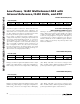
FIRST BIT (MSB) (LSB)
NAME WU2 WU1 RST LVD SDC CLK ADD —
DEFAULT 0 0 1 1 0 0 0 0
STATUS REGISTER (00110)
Table 6. BCD Conversion
DECIMAL DIGIT BCD
0 0000
1 0001
2 0010
3 0011
4 0100
5 0101
6 0110
7 0111
8 1000
9 1001
UNUSED CODES
1010
1011
1100
1101
1110
1111