
Datasheet


MAX1403
+3V, 18-Bit, Low-Power, Multichannel,
Oversampling (Sigma-Delta) ADC
______________________________________________________________________________________ 17
exact sequence depends on the state of the DIFF bit
(Table 4). When scanning, the calibration channels use
the PGA gain, format, and DAC settings defined by the
contents of Transfer Function Register 3.
BUFF: (Default = 0) The BUFF bit controls operation of
the input buffer amplifiers. When this bit is 0, the inter-
nal buffers are bypassed and powered down. When
this bit is set high, the buffers drive the input sampling
capacitors and minimize the dynamic input load.
DIFF: (Default = 0) Differential/Pseudo-Differential Bit.
When DIFF = 0, the part is in pseudo-differential mode,
and AIN1–AIN5 are measured respective to AIN6, the
analog common. When DIFF = 1, the part is in differen-
tial mode with the analog inputs defined as AIN1/AIN2,
AIN3/AIN4, and AIN5/AIN6. The available input chan-
nels for each mode are tabulated in Table 5. Note that
DIFF also affects the scanning sequence when the part
is placed in SCAN mode (Table 4).
BOUT: (Default = 0) Burn-Out Current Bit. Setting BOUT
= 1 connects 100nA current sources to the selected ana-
log input channel. This mode is used to check that a
transducer has not burned out or opened circuit. The
burn-out current source must be turned off (BOUT = 0)
before measurement to ensure best linearity.
IOUT: (Default = 0) The IOUT bit controls the
Transducer Excitation Currents. A 0 in this bit disables
OUT1 and OUT2, effectively making these pins high-
impedance. A 1 in this location activates both IOUT1
and IOUT2, causing each pin to source 200µA.
X2CLK: (Default = 0) Times-Two Clock Bit. Setting this
bit to 1 selects a divide-by-2 prescaler in the clock sig-
nal path. This allows use of a higher frequency crystal
or clock source and improves immunity to asymmetric
clock sources.
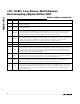
Table 2. Data Output Rate vs. CLK, Filter Select, and Modulator Frequency Bits
* Data rates offering noise-free 16-bit resolution.
Note: When FAST = 0, f
-3dB
= 0.262 · Data Rate. When FAST = 1, f
-3dB
= 0.443 · Data Rate.
Note: Default condition is in bold print.
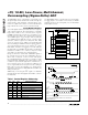
Table 3. Special Modes Controlled by M1, M0 (SCAN = 0)
DESCRIPTIONM1
0
1
Normal Mode: The device operates normally.
Calibrate Gain: In this mode, the MAX1403 converts the voltage applied across CALGAIN+
and CALGAIN-. The PGA gain, DAC, and format settings of the selected channel (defined by
DIFF, A1, A0) are used.
1
Reserved: Do not use.
1
0
0
Calibrate Offset: In this mode, the MAX1403 converts the voltage applied across CALOFF+
and CALOFF-. The PGA gain, DAC, and format settings of the selected channel (defined by
DIFF, A1, A0) are used.
1
M0
0
2400 4800400 480114.9152 12.4576
1200 2400200 240114.9152 02.4576
600 1200100 120014.9152 12.4576
300 60050
6001
4.9152
02.4576
800 1600160 200102.048 11.024
400 80080 100102.048 01.024
200 40040 50002.048 11.024
100
X2CLK = 0
20020 2500
X2CLK = 1
2.048 0
CLKIN FREQUENCY,
f
CLKIN
(MHz)
1.024
FS1, FS0*
(0, 0)
FS1, FS0*
(0, 1)
FS1, FS0
(1, 0)
FS1, FS0
(1, 1)
AVAILABLE OUTPUT DATA RATES
(sps)
CLK MF1 MF0