
Datasheet


Detailed Description
The MAX1329/MAX1330 smart DASs are based on a
312ksps, 12-bit SAR ADC with a 1ksps, 16-bit DSP
mode. The ADC includes a differential multiplexer, a pro-
grammable gain amplifier (PGA) with gains of 1, 2, 4,
and 8, a 20-bit accumulator, internal dither, a 16-word
FIFO, and an alarm register. The MAX1329/MAX1330
operate with a digital supply down to 1.8V and feature an
internal charge pump to boost the supply voltage for the
analog circuitry that requires 2.7V to 5.5V.
The MAX1329/MAX1330 include an internal reference
with programmable buffer for the ADC, two analog exter-
nal inputs as well as inputs from other internal circuitry,
an internal/external temperature sensor, internal oscilla-
tor, dual single-pole, double-throw (SPDT) switches, four
digital programmable I/Os, four analog programmable
I/Os, and dual programmable voltage monitors.
The MAX1329 features dual 12-bit force-sense DACs
with programmable reference buffer and one opera-
tional amplifier. The MAX1330 includes one 12-bit force-
sense DAC with programmable reference buffer and
dual op amps. DACA can be sequenced with a 16-word
FIFO. The DAC buffers and op amps have internal ana-
log switches between the output and the inverting input.
Power-On Reset
After a power-on reset, the DV
DD
voltage supervisor is
enabled with thresholds at 1.8V and 2.7V. All digital
and analog programmable I/Os (DPIOs and APIOs) are
configured as inputs with pullups enabled. The internal
oscillator is enabled and is output at CLKIO once the
1.8V reset trip threshold has been exceeded and the
subsequent timeout period has expired. See the
Register Bit Descriptions
section for the default values
after a power-on reset.
Power-On Setup
After applying power to AV
DD
:
1) Write to the Reset register. This initializes the tem-
perature sensor and voltage reference trim logic.
2) Within 3ms following the reset, configure the charge
pump as desired by writing to the CP/VM Control
register. The details of programming the charge
pump are described in the
Charge Pump
section.
Charge Pump
Power AV
DD
and DV
DD
by any one of the following
ways: drive AV
DD
and DV
DD
with a single external
power supply, drive AV
DD
and DV
DD
with separate
external power supplies, or drive DV
DD
with an external
supply and enable the internal charge pump to gener-
ate AV
DD
or short DV
DD
to AV
DD
internally.
MAX1329/MAX1330
12-/16-Bit DASs with ADC, DACs, DPIOs, APIOs,
Reference, Voltage Monitors, and Temp Sensor
______________________________________________________________________________________ 25
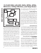
t
DS
t
CSS
t
DH
t
DV
t
DO
t
TR
CS
SCLK
DIN
DOUT
t
CSH
t
CYC
t
CH
t
CL
t
CSH
Figure 1. Detailed Serial-Interface Timing Diagram
DV
DD
C
LOAD
= 20pF
3kΩ
DOUT
a) FOR ENABLE, HIGH IMPEDANCE
TO V
OH
AND V
OL
TO V
OH
.
FOR DISABLE, V
OH
TO HIGH IMPEDANCE.
b) FOR ENABLE, HIGH IMPEDANCE
TO V
OL
AND V
OH
TO V
OL
.
FOR DISABLE, V
OL
TO HIGH IMPEDANCE.
DOUT
3kΩ
C
LOAD
= 20pF
Figure 2. DOUT Enable and Disable Time Load Circuits