
Datasheet


+5.0V, ±15kV ESD-Protected, Fail-Safe,
Hot-Swap, RS-485/RS-422 Transceivers
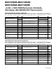
DRIVER SWITCHING CHARACTERISTICS
MAX13086E/MAX13087E/MAX13088E/MAX13089E WITH SRL = GND (16Mbps)
(V
CC
= +5.0V ±10%, T
A
= T
MIN
to T
MAX
, unless otherwise noted. Typical values are at V
CC
= +5.0V and T
A
= +25°C.)
PARAMETER SYMBOL CONDITIONS MIN TYP MAX UNITS
t
DPLH
50
Driver Propagation Delay
t
DPHL
C
L
= 50pF, R
L
= 54Ω, Figures 2 and 3
50
ns
Driver Differential Output Rise or
Fall Time
t
R ,
t
F
C
L
= 50pF, R
L
= 54Ω, Figures 2 and 3 15 ns
Differential Driver Output Skew
|t
DPLH
- t
DPHL
|
t
DSKEW
C
L
= 50pF, R
L
= 54Ω, Figures 2 and 3 8 ns
Maximum Data Rate 16 Mbps
Driver Enable to Output High t
DZH
Figure 4 150 ns
Driver Enable to Output Low t
DZL
Figure 5 150 ns
Driver Disable Time from Low t
DLZ
Figure 5 100 ns
Driver Disable Time from High t
DHZ
Figure 4 100 ns
Driver Enable from Shutdown to
Output High
t
DZH
(
SHDN
)
Figure 4 2200 ns
Driver Enable from Shutdown to
Output Low
t
DZL
(
SHDN
)
Figure 5 2200 ns
Time to Shutdown t
SHDN
50 340 700 ns
RECEIVER SWITCHING CHARACTERISTICS
MAX13086E/MAX13087E/MAX13088E/MAX13089E WITH SRL = GND (16Mbps)
(V
CC
= +5.0V ±10%, T
A
= T
MIN
to T
MAX
, unless otherwise noted. Typical values are at V
CC
= +5.0V and T
A
= +25°C.)
PARAMETER SYMBOL CONDITIONS MIN TYP MAX UNITS
t
RPLH
50 80
Receiver Propagation Delay
t
RPHL
C
L
= 15pF, Figures 6 and 7
50 80
ns
Receiver Output Skew
|t
RPLH
- t
RPHL
|
t
RSKEW
C
L
= 15pF, Figures 6 and 7 13 ns
Maximum Data Rate 16 Mbps
Receiver Enable to Output Low t
RZL
Figure 8 50 ns
Receiver Enable to Output High t
RZH
Figure 8 50 ns
Receiver Disable Time from Low t
RLZ
Figure 8 50 ns
Receiver Disable Time from High t
RHZ
Figure 8 50 ns
Receiver Enable from Shutdown
to Output High
t
RZH
(
SHDN
)
Figure 8 2200 ns
Receiver Enable from Shutdown
to Output Low
t
RZL
(
SHDN
)
Figure 8 2200 ns
Time to Shutdown t
SHDN
50 340 700 ns
Note 1: All currents into the device are positive. All currents out of the device are negative. All voltages are referred to device ground,
unless otherwise noted.
Note 2: ΔV
OD
and ΔV
OC
are the changes in V
OD
and V
OC
, respectively, when the DI input changes state.
Note 3: The short-circuit output current applies to peak current just prior to foldback current limiting. The short-circuit foldback output
current applies during current limiting to allow a recovery from bus contention.
6
Maxim Integrated
MAX13080E–MAX13084E/
MAX13086E–MAX13089E