
Datasheet


Mode Control
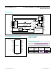
The MAX1300/MAX1301 contain one byte-wide mode-
control register. The timing diagram of Figure 15 shows
how to use the mode-control byte, and the mode-control
byte format is shown in Table 7. The mode-control byte is
used to select the conversion method and to control the
power modes of the MAX1300/MAX1301.
Selecting the Conversion Method
The conversion method is selected using the mode-con-
trol byte (see the Mode Control section), and the conver-
sion is initiated using a conversion-start command (Table
3, and Figures 2, 3, and 4).The MAX1300/MAX1301
convert analog signals to digital data using one of three
methods:
• External Clock Mode, Mode 0 (Figure 2)
• Highest maximum throughput (see the Electrical
Characteristics table)
• User controls the sample instant
• CS remains low during the conversion
•
User supplies SCLK throughout the ADC conversion
and reads data at DOUT
• External Acquisition Mode, Mode 1 (Figure 3)
• Lowest maximum throughput (see the Electrical
Characteristics table)
• User controls the sample instant
• User supplies two bytes of SCLK, then drives
CS high to relieve processor load while the ADC
converts
• After SSTRB transitions high, the user supplies
two bytes of SCLK and reads data at DOUT
• Internal Clock Mode, Mode 2 (Figure 4)
• High maximum throughput (see the Electrical
Characteristics table)
Figure 12. Ideal Bipolar Transfer Function, Single-Ended or
Differential Input
Figure 14. Ideal Unipolar Transfer Function, Single-Ended
Input, 0 to +FSR
Figure 13. Ideal Unipolar Transfer Function, Single-Ended
Input, -FSR to 0
1 LSB =
FSR x V
REF
65,536 x 4.096V
BINARY OUTPUT CODE (LSB [hex])
FFFF
FFFE
FFFD
8001
8000
7FFF
0003
0002
0001
0000
FSR
-32,768 -32,766 0 +32,765 +32,767
INPUT VOLTAGE (LSB [DECIMAL])
AGND1 (DIF/SGL = 0)
OV (DIF/SGL = 1)
FSR
-1 +1
1 LSB =
FSR x V
REF
65,536 x 4.096V
BINARY OUTPUT CODE (LSB [hex])
FFFF
FFFE
FFFD
8001
8000
7FFF
0003
0002
0001
0000
FSR
0 1 2 3 32,768 65,533 65,535
INPUT VOLTAGE (LSB [DECIMAL])
(AGND1)
FSR
1 LSB =
FSR x V
REF
65,536 x 4.096V
BINARY OUTPUT CODE (LSB [hex])
FFFF
FFFE
FFFD
8001
8000
7FFF
0003
0002
0001
0000
FSR
0 1 2 3 32,768 65,533 65,535
INPUT VOLTAGE (LSB [DECIMAL])
(AGND1)
FSR
MAX1300/MAX1301 8- and 4-Channel, ±3 x V
REF
Multirange Inputs,
Serial 16-Bit ADCs
www.maximintegrated.com
Maxim Integrated
│
22