
Datasheet
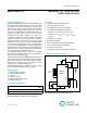


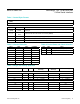

Table 1. Control-Byte Format
Table 3. Range and Polarity Selection
Table 2. Channel Selection Table 4. Power-Down and Clock Selection
BIT 7
(MSB)
BIT 6 BIT 5 BIT 4 BIT 3 BIT 2 BIT 1 BIT 0
START SEL2 SEL1 SEL0 RNG BIP PD1 PD0
BIT NAME DESCRIPTION
7 (MSB) START
The logic “1” received after acknowledge of a write bit (R/W = 0) denes the beginning of the
control byte.
6, 5, 4
SEL2, SEL1,
SEL0
These three bits select the desired “ON” channel (Table 2).
3 RNG Selects the full-scale input voltage range (Table 3).
2 BIP Selects unipolar or bipolar conversion mode (Table 3).
1, 0 (LSB) PD1, PD0 These two bits select the power-down modes (Table 4).
SEL2 SEL1 SEL0 CHANNEL
0 0 0 CH0
0 0 1 CH1
0 1 0 CH2
0 1 1 CH3
1 0 0 CH4
1 0 1 CH5
1 1 0 CH6
1 1 1 CH7
PD1 PD0 SEL0
0 X Normal Operation (always on)
1 0 Standby Power-Down Mode (STBYPD)
1 1 Full Power-Down Mode (FULLPD)
INPUT RANGE (V) RNG BIP
NEGATIVE FULL
SCALE (V)
ZERO
SCALE (V)
FULL SCALE (V)
MAX127
0 to 5 0 0 — 0 V
REF
x 1.2207
0 to 10 1 0 — 0 V
REF
x 2.4414
±5 0 1 -V
REF
x 1.2207 0 V
REF
x 1.2207
±10 1 1 -V
REF
x 2.4414 0 V
REF
x 2.4414
MAX128
0 to V
REF
/2 0 0 — 0 V
REF
/2
0 to V
REF
1 0 — 0 V
REF
±V
REF
/2 0 1 -V
REF
/2 0 V
REF
/2
±V
REF
1 1 -V
REF
0 V
REF
MAX127/MAX128 Multirange, +5V, 12-Bit DAS with
2-Wire Serial Interface
www.maximintegrated.com
Maxim Integrated
│
10