
Datasheet


and a trailing zero with the data in MSB-first format.
DSP Interface to the TMS320C54_
The MAX1276/MAX1278 can be directly connected
to the TMS320C54_ family of DSPs from Texas
Instruments, Inc. Set the DSP to generate its own
clocks or use external clock signals. Use either the
standard or buffered serial port. Figure 15 shows the
simplest interface between the MAX1276/MAX1278 and
the TMS320C54_, where the transmit serial clock
(CLKX) drives the receive serial clock (CLKR) and
SCLK, and the transmit frame sync (FSX) drives the
receive frame sync (FSR) and CNVST.
For continuous conversion, set the serial port to trans-
mit a clock, and pulse the frame sync signal for a clock
period before data transmission. The serial-port config-
uration (SPC) register should be set up with internal
frame sync (TXM = 1), CLKX driven by an on-chip clock
source (MCM = 1), burst mode (FSM = 1), and 16-bit
word length (FO = 0).
This setup allows continuous conversions provided that
the data-transmit register (DXR) and the data-receive
register (DRR) are serviced before the next conversion.
Alternatively, autobuffering can be enabled when using
the buffered serial port to execute conversions and
MAX1276/MAX1278
1.8Msps, Single-Supply, Low-Power, True-
Differential, 12-Bit ADCs with Internal Reference
14 ______________________________________________________________________________________
SCLK
DOUT
916
8
1
D2
D11
D10
D8
D7
D6
D5
D4
D3
D9
HIGH-Z
HIGH-Z
CNVST
D1
D0
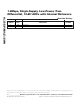
Figure 13. SPI/MICROWIRE Serial-Interface Timing—Continuous Conversion (CPOL = CPHA = 0), (CPOL = CPHA = 1)
0 0 0 D11 D10 D9 D8 D7 D6 D5 D4 D3 D2 D1 D0 0
DOUT
SCLK
CNVST
0
1
1
14
16
Figure 12. SPI/MICROWIRE Serial-Interface Timing—Single Conversion (CPOL = CPHA = 0), (CPOL = CPHA = 1)
Figure 14. QSPI Serial-Interface Timing—Single Conversion (CPOL = 1, CPHA = 1)
SCLK
DOUT
CNVST
16
D0
D1
D11
D10
D6D7D8 D5 D4 D3 D2
HIGH-Z
D9
HIGH-Z
2