
Datasheet


Input Range and Protection
The MAX1272/MAX1273 provide software-selectable
analog input voltage ranges. Program the analog input
to one of four ranges by setting the appropriate control
bits (RNG, BIP) in the control byte (Table 1). The
MAX1272 has selectable input voltage ranges extend-
ing to ±10V (±V
REF
2.4414), while the MAX1273 has
selectable input voltage ranges extending to ±V
REF
.
Figure 3 shows the equivalent input circuit.
Overvoltage circuitry at the analog input provides ±12V
fault protection for the MAX1272. This circuit limits the
current going into or out of the device to less than 2mA,
providing an added layer of protection from momentary
over/undervoltages at the analog input. The overvoltage
protection activates when the device enters power-
down mode or if V
DD
= 0V.
MAX1272/MAX1273
Fault-Protected, 12-Bit ADCs
with Software-Selectable Input Range
_______________________________________________________________________________________ 9
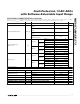
DIN DOUT SCLK
AIN
REF
V
DD
GND
SERIAL INTERFACE
LOGIC
SIGNAL
CONDITIONING
4.096V
REFERENCE
T/H
12-BIT
SAR ADC
CS
REF
IN
OUT
CLK
MAX1272
MAX1273
Figure 2. Simplified Block Diagram
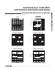
BIT 7
(MSB)
BIT 6 BIT 5 BIT 4 Bit 3 BIT 2 BIT 1
BIT 0
(LSB)
START RNG BIP PD MODE1 MODE0 RESERVED REF
BIT NAME DESCRIPTION
7 (MSB) START Write a logic 1 (see the Input Data Format section)
6 RNG Selects the full-scale input voltage range (Tables 2, 3)
5 BIP Selects unipolar or bipolar conversion mode (Tables 2, 3)
4 PD Selects normal operation (PD = 1) or power-down (PD = 0) mode
3 MODE1 Selects standby power-down (STBYPD) or full power-down (FULLPD) mode (Table 4)
2 MODE0 Selects delayed or immediate power-down mode (Table 4)
1 RESERVED Write a logic 0
0 (LSB) REF Selects external (REF = 0, default) or internal (REF = 1) reference mode
Table 1. Control-Byte Format