
Datasheet


MAX1248/MAX1249
+2.7V to +5.25V, Low-Power, 4-Channel,
Serial 10-Bit ADCs in QSOP-16
2 _______________________________________________________________________________________
ABSOLUTE MAXIMUM RATINGS
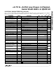
ELECTRICAL CHARACTERISTICS
(V
DD
= +2.7V to +5.25V; COM = 0V; f
SCLK
= 2.0MHz; external clock (50% duty cycle); 15 clocks/conversion cycle (133ksps);
MAX1248—4.7µF capacitor at VREF pin; MAX1249—external reference, VREF = 2.500V applied to VREF pin; T
A
= T
MIN
to T
MAX
,
unless otherwise noted.)
Stresses beyond those listed under “Absolute Maximum Ratings” may cause permanent damage to the device. These are stress ratings only, and functional
operation of the device at these or any other conditions beyond those indicated in the operational sections of the specifications is not implied. Exposure to
absolute maximum rating conditions for extended periods may affect device reliability.
V
DD
to AGND, DGND.............................................. -0.3V to +6V
AGND to DGND.................................................... -0.3V to +0.3V
CH0–CH3, COM to AGND, DGND............ -0.3V to (V
DD
+ 0.3V)
VREF to AGND........................................... -0.3V to (V
DD
+ 0.3V)
Digital Inputs to DGND............................................ -0.3V to +6V
Digital Outputs to DGND........................... -0.3V to (V
DD
+ 0.3V)
Digital Output Sink Current.................................................25mA
Continuous Power Dissipation (T
A
= +70°C)
Plastic DIP (derate 10.53mW/°C above +70°C) ......... 842mW
QSOP (derate 8.30mW/°C above +70°C)................... 667mW
CERDIP (derate 10.00mW/°C above +70°C).............. 800mW
Operating Temperature Ranges
MAX1248_C_E/MAX1249_C_E.......................... 0°C to +70°C
MAX1248_E_E/MAX1249_E_E........................ -40°C to +85°C
MAX1248_MJE/MAX1249_MJE.................... -55°C to +125°C
Storage Temperature Range............................ -60°C to +150°C
Lead Temperature (soldering, 10sec)............................ +300°C
6
µs
35 65
t
CONV
Conversion Time (Note 5)
5.5 7.5
MHz1.0Full-Power Bandwidth
MHz2.25Small-Signal Bandwidth
dB-75Channel-to-Channel Crosstalk
dB70SFDRSpurious-Free Dynamic Range
dB-70THDTotal Harmonic Distortion
dB66SINADSignal-to-Noise + Distortion Ratio
LSB±0.05
Channel-to-Channel Offset
Matching
ppm/°C±0.25Gain Temperature Coefficient
±0.5
Bits10Resolution
±1
Offset Error
LSB
±1.0
INLRelative Accuracy (Note 2)
LSB±1DNL
±1
LSB
±2
UNITSMIN TYP MAXSYMBOLPARAMETER
External clock = 2MHz, 12 clocks/conversion
Internal clock, SHDN = V
DD
Internal clock, SHDN = FLOAT
MAX124_A
-3dB rolloff
65kHz, 2.500Vp-p (Note 4)
Up to the 5th harmonic
MAX124_A
MAX124_B
No missing codes over temperature
MAX124_A
MAX124_B
CONDITIONS
Differential Nonlinearity
ns30Aperture Delay
MHz
1.8
SHDN = FLOAT
ps<50Aperture Jitter
MHz
0.1 2.0
µs1.5t
ACQ
Track/Hold Acquisition Time
0.225
Internal Clock Frequency
SHDN = V
DD
0 2.0
External Clock Frequency
Data transfer only
LSBGain Error (Note 3)
±2MAX124_B
DC ACCURACY (Note 1)
DYNAMIC SPECIFICATIONS (10kHz sine-wave input, 0V to 2.500Vp-p, 133ksps, 2.0MHz external clock, bipolar input mode)
CONVERSION RATE