
Datasheet


MAX1204
5V, 8-Channel, Serial, 10-Bit ADC
with 3V Digital Interface
3
Maxim Integrated
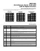
ELECTRICAL CHARACTERISTICS (continued)
(V
DD
= +5V ±5%, V
L
= 2.7V to 3.6V; V
SS
= 0V or -5V ±5%; f
SCLK
= 2.0MHz, external clock (50% duty cycle); 15 clocks/conversion
cycle (133ksps); 4.7µF capacitor at REF; T
A
= T
MIN
to T
MAX
; unless otherwise noted.)
MAX1204AC
T
A
= +25°C
External clock, 2MHz, 12 clocks/conversion
(Note 6)
On/off leakage current, V
CH_
= ±5V
Bipolar, V
SS
= -5V
Unipolar, V
SS
= 0V
6
Used for data transfer only
Internal compensation mode (Note 6)
Internal clock
External compensation mode, 4.7µF
CONDITIONS
ppm/°C
±30 ±50
V
REF
Temperature Coefficient
mA30REF Short-Circuit Current
V4.076 4.096 4.116REF Output Voltage
pF16Input Capacitance
µA±0.01 ±1Multiplexer Leakage Current
±V
REF
/2
V
V
REF
Input Voltage Range, Single-
Ended and Differential (Note 7)
0 2.0
0.1 0.4
MHz
0.1 2.0
External Clock-Frequency Range
MHz1.7Internal Clock Frequency
ns10Aperture Delay
µs1.5t
ACQ
Track/Hold Acquisition Time
µs
5.5 10
t
CONV
Conversion Time (Note 5)
UNITSMIN TYP MAXSYMBOLPARAMETER
MAX1204AE ±30 ±60
±30MAX1204B
0mA to 0.5mA output load mV2.5Load Regulation (Note 8)
Internal compensation mode
µF
0
Capacitive Bypass at REF
External compensation mode 4.7
µF0.01Capacitive Bypass at REFADJ
%±1.5REFADJ Adjustment Range
V
2.50 V
DD
+
50mV
Input Voltage Range
µA200 350Input Current
kΩ12 20Input Resistance
V
SHDN
= 0V
µA1.5 10REF Input Current in Shutdown
V
V
DD
-
50mV
REFADJ Buffer Disable Threshold
ps<50Aperture Jitter
CONVERSION RATE
INTERNAL REFERENCE
ANALOG INPUT
EXTERNAL REFERENCE AT REF (Buffer disabled, V
REF
= 4.096V)