
Datasheet


MAX1191
Ultra-Low-Power, 7.5Msps, Dual 8-Bit ADC
______________________________________________________________________________________ 15
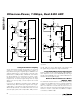
Input Track-and-Hold (T/H) Circuits
Figure 3 displays a simplified functional diagram of the
input T/H circuits. In track mode, switches S1, S2a,
S2b, S4a, S4b, S5a, and S5b are closed. The fully dif-
ferential circuits sample the input signals onto the two
capacitors (C2a and C2b) through switches S4a and
S4b. S2a and S2b set the common mode for the ampli-
fier input, and open simultaneously with S1, sampling
the input waveform. Switches S4a, S4b, S5a, and S5b
are then opened before switches S3a and S3b connect
capacitors C1a and C1b to the output of the amplifier
and switch S4c is closed. The resulting differential volt-
ages are held on capacitors C2a and C2b. The ampli-
fiers charge capacitors C1a and C1b to the same
S3b
S3a
COM
S5b
S5a
INB+
INB-
S1
OUT
OUT
C2a
C2b
S4c
S4a
S4b
C1b
C1a
INTERNAL
BIAS
INTERNAL
BIAS
COM
HOLD
HOLD
CLK
INTERNAL
NONOVERLAPPING
CLOCK SIGNALS
TRACK
TRACK
S2a
S2b
S3b
S3a
COM
S5b
S5a
INA+
INA-
S1
OUT
OUT
C2a
C2b
S4c
S4a
S4b
C1b
C1a
INTERNAL
BIAS
INTERNAL
BIAS
COM
S2a
S2b
MAX1191
Figure 3. Internal T/H Circuits