
Datasheet


Conversion Register
Select active analog input channels per scan and scan
modes by writing to the conversion register. Table 2
details channel selection and the four scan modes.
Request a scan by writing to the conversion register when
in clock mode 10 or 11, or by applying a low pulse to the
CNVST pin when in clock mode 00 or 01.
A conversion is not performed if it is requested on a chan-
nel that has been configured as CNVST. Do not request
conversions on channels 8–15 on the MAX11626–
MAX11629. Set CHSEL3:CHSEL0 to the lower channel’s
binary values.
Select scan mode 00 or 01 to return one result per single-
ended channel within the requested range. Select scan
mode 10 to scan a single input channel numerous times,
depending on NSCAN1 and NSCAN0 in the averaging
register (Table 4). Select scan mode 11 to return only one
result from a single channel.
Setup Register
Write a byte to the setup register to configure the clock,
reference, and power-down modes. Table 3 details the
bits in the setup register. Bits 5 and 4 (CKSEL1 and
CKSEL0) control the clock mode, acquisition and sam-
pling, and the conversion start. Bits 3 and 2 (REFSEL1
and REFSEL0) control internal or external reference use.
Averaging Register
Write to the averaging register to configure the ADC to
average up to 32 samples for each requested result, and
to independently control the number of results requested
for single-channel scans.
Table 2 details the four scan modes available in the con-
version register. All four scan modes allow averaging as
long as the AVGON bit, bit 4 in the averaging register, is
set to 1. Select scan mode 10 to scan the same channel
multiple times. Clock mode 11 disables averaging.
Reset Register
Write to the reset register (as shown in Table 5) to clear
the FIFO or to reset all registers to their default states.
Set the RESET bit to 1 to reset the FIFO. Set the reset bit
to zero to return the MAX11626–MAX11629/MAX11632/
MAX11633 to the default power-up state.
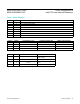
Table 2. Conversion Register*
*See below for bit details.
BIT
NAME
BIT FUNCTION
— 7 (MSB) Set to 1 to select conversion register.
CHSEL3 6 Analog input channel select.
CHSEL2 5 Analog input channel select.
CHSEL1 4 Analog input channel select.
CHSEL0 3 Analog input channel select.
SCAN1 2 Scan mode select.
SCAN0 1 Scan mode select.
— 0 (LSB) Don’t care.
CHSEL3 CHSEL2 CHSEL1 CHSEL0
SELECTED
CHANNEL (N)
0 0 0 0 AIN0
0 0 0 1 AIN1
0 0 1 0 AIN2
0 0 1 1 AIN3
0 1 0 0 AIN4
0 1 0 1 AIN5
0 1 1 0 AIN6
0 1 1 1 AIN7
1 0 0 0 AIN8
1 0 0 1 AIN9
1 0 1 0 AIN10
1 0 1 1 AIN11
1 1 0 0 AIN12
1 1 0 1 AIN13
1 1 1 0 AIN14
1 1 1 1 AIN15
SCAN1 SCAN0
SCAN MODE (CHANNEL N IS
SELECTED BY BITS chsel3–chsel0)
0 0 Scans channels 0 through N.
0 1
Scans channels N through the highest
numbered channel.
1 0
Scans channel N repeatedly. The averaging
register sets the number of results.
1 1 No scan. Converts channel N once only.
MAX11626–MAX11629/
MAX11632/MAX11633
12-Bit, 300ksps ADCs
with FIFO and Internal Reference
www.maximintegrated.com
Maxim Integrated
│
14