
Datasheet


MAX11618–MAX11621/MAX11624/MAX11625
10-Bit, 300ksps ADCs
with FIFO and Internal Reference
4 _______________________________________________________________________________________
Note 2: Limits at T
A
= -40°C are guaranteed by design and not production tested.
Note 3: MAX11619/MAX11621/MAX11625 tested at V
DD
= +3V. MAX11618/MAX11620/MAX11624 tested at V
DD
= +5V.
Note 4: Offset nulled.
Note 5: Time for reference to power up and settle to within 1 LSB.
Note 6: Conversion time is defined as the number of clock cycles multiplied by the clock period; clock has 50% duty cycle.
Note 7: See Figure 3 (Equivalent Input Circuit) and the Sampling Error vs. Source Impedance curve in the
Typical Operating
Characteristics
section.
Note 8: When CNVST is configured as a digital input, do not apply a voltage between V
IL
and V
IH
.
Note 9: Supply current is specified depending on whether an internal or external reference is used for voltage conversions.
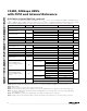
ELECTRICAL CHARACTERISTICS (continued)
(V
DD
= 2.7V to 3.6V (MAX11619/MAX11621/MAX11625); V
DD
= 4.75V to 5.25V (MAX11618/MAX11620/MAX11624),
f
SAMPLE
= 300kHz, f
SCLK
= 4.8MHz (external clock, 50% duty cycle), V
REF
= 2.5V (MAX11619//MAX11621/MAX11625); V
REF
= 4.096V
(MAX11618/MAX11620/MAX11624), T
A
= T
MIN
to T
MAX
, unless otherwise noted. Typical values are at T
A
= +25°C.) (Note 2)
PARAMETER SYMBOL CONDITIONS MIN TYP MAX UNITS
DIGITAL INPUTS (SCLK, DIN, CS, CNVST) (Note 8)
MAX11618/MAX11620/MAX11624 0.8
Input-Voltage Low V
IL
MAX11619/MAX11621/MAX11625 V
DD
x 0.3
V
MAX11618/MAX11620/MAX11624 2.0
Input-Voltage High V
IH
MAX11619/MAX11621/MAX11625 V
DD
x 0.7
V
Input Hysteresis V
HYST
200 mV
Input Leakage Current I
IN
V
IN
= 0V or V
DD
±0.01 ±1.0 µA
Input Capacitance C
IN
15 pF
DIGITAL OUTPUTS (DOUT, EOC)
I
SINK
= 2mA 0.4
Output-Voltage Low V
OL
I
SINK
= 4mA 0.8
V
Output-Voltage High V
OH
I
SOURCE
= 1.5mA V
DD
- 0.5 V
Three-State Leakage Current I
L
CS = V
DD
±0.05 ±1 µA
Three-State Output
C
OUT
CS = V
DD
15 pF
POWER REQUIREMENTS
MAX11618/MAX11620/MAX11624 4.75 5.25
Supply Voltage V
DD
MAX11619/MAX11621/MAX11625 2.7 3.6
V
f
SAMPLE
= 300ksps 1750 2000
f
SAMPLE
= 0, REF on 1000 1200
Internal reference
Shutdown 0.2 5
f
SAMPLE
= 300ksps 1050 1200
MAX11619/MAX11621/
MAX11625 Supply Current
(Note 9)
I
DD
External reference
Shutdown 0.2 5
µA
f
SAMPLE
= 300ksps 2300 2550
f
SAMPLE
= 0, REF on 1000 1350
Internal reference
Shutdown 0.2 5
f
SAMPLE
= 300ksps 1550 1700
MAX11618/MAX11620/
MAX11624 Supply Current
(Note 9)
I
DD
External reference
Shutdown 0.2 5
µA
V
DD
= 2.7V to 3.6V, full-scale input ±0.2 ±1
Power-Supply Rejection PSR
V
DD
= 4.75V to 5.25V, full-scale input ±0.2 ±1.4
mV