
Datasheet


MAX11618–MAX11621/MAX11624/MAX11625
10-Bit, 300ksps ADCs
with FIFO and Internal Reference
2 _______________________________________________________________________________________
ABSOLUTE MAXIMUM RATINGS
ELECTRICAL CHARACTERISTICS
(V
DD
= 2.7V to 3.6V (MAX11619/MAX11621/MAX11625); V
DD
= 4.75V to 5.25V (MAX11618/MAX11620/MAX11624),
f
SAMPLE
= 300kHz, f
SCLK
= 4.8MHz (external clock, 50% duty cycle), V
REF
= 2.5V (MAX11619//MAX11621/MAX11625); V
REF
= 4.096V
(MAX11618/MAX11620/MAX11624), T
A
= T
MIN
to T
MAX
, unless otherwise noted. Typical values are at T
A
= +25°C.) (Note 2)
Stresses beyond those listed under “Absolute Maximum Ratings” may cause permanent damage to the device. These are stress ratings only, and functional
operation of the device at these or any other conditions beyond those indicated in the operational sections of the specifications is not implied. Exposure to
absolute maximum rating conditions for extended periods may affect device reliability.
V
DD
to GND..............................................................-0.3V to +6V
CS, SCLK, DIN, EOC, DOUT to GND.........-0.3V to (V
DD
+ 0.3V)
AIN0–AIN14, CNVST/AIN_,
REF to GND...........................................-0.3V to (V
DD
+ 0.3V)
Maximum Current into Any Pin............................................50mA
Continuous Power Dissipation (T
A
= +70°C)
16-Pin QSOP (derate 8.3mW/°C above +70°C)...........667mW
24-Pin QSOP (derate 9.5mW/°C above +70°C)...........762mW
Operating Temperature Range ...........................-40°C to +85°C
Storage Temperature Range .............................-60°C to +150°C
Junction Temperature......................................................+150°C
Lead Temperature (soldering, 10s) .................................+300°C
Soldering Temperature (reflow) .......................................+260°C
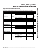
PARAMETER SYMBOL CONDITIONS MIN TYP MAX UNITS
DC ACCURACY (Note 3)
Resolution RES 10 Bits
Integral Nonlinearity INL ±1.0 LSB
Differential Nonlinearity DNL No missing codes over temperature ±1.0 LSB
Offset Error ±0.5 ±2.0 LSB
Gain Error (Note 4) ±0.5 ±2.0 LSB
Offset Error Temperature
Coefficient
±2
ppm/°C
FSR
Gain Temperature Coefficient ±0.8 ppm/°C
Channel-to-Channel Offset
Matching
±0.1 LSB
DYNAMIC SPECIFICATIONS (30kHz sine-wave input, 300ksps, f
SCLK
= 4.8MHz)
Signal-to-Noise Plus Distortion SINAD 62 dB
Total Harmonic Distortion THD Up to the 5th harmonic -79 dBc
Spurious-Free Dynamic Range SFDR -81 dBc
Intermodulation Distortion IMD f
IN1
= 29.9kHz, f
IN2
= 30.1kHz -74 dBc
Full-Power Bandwidth -3dB point 1 MHz
Full-Linear Bandwidth S/(N + D) > 61dB 100 kHz
Note 1: Package thermal resistances were obtained usiˇng the method described in JEDEC specification JESD51-7, using a four-
layer board. For detailed information on package thermal considerations, refer to www.maxim-ic.com/thermal-tutorial
.
PACKAGE THERMAL CHARACTERISTICS (Note 1)
16 QSOP
Junction-to-Ambient Thermal Resistance (θ
JA
)...............105°C/W
Junction-to-Case Thermal Resistance (θ
JC
)......................37°C/W
24 QSOP
Junction-to-Ambient Thermal Resistance (θ
JA
)................88°C/W
Junction-to-Case Thermal Resistance (θ
JC
).......................34°C/W