
Datasheet


MAX11047–MAX11049/MAX11057–MAX11059
4-/6-/8-Channel, 16-/14-Bit,
Simultaneous-Sampling ADCs
14 ______________________________________________________________________________________
Detailed Description
The MAX11047/MAX11048/MAX11049 and MAX11057/
MAX11058/MAX11059 are fast, low-power ADCs that
combine 4, 6, or 8 independent ADC channels in a sin-
gle IC. Each channel includes simultaneously sampling
independent T/H circuitry that preserves relative phase
information between inputs making the devices ideal for
motor control and power monitoring. The devices are
available with a 0 to 5V input range that features
±20mA overrange, fault-tolerant inputs. The devices
operate with a single 4.75V to 5.25V supply. A separate
2.7V to 5.25V supply for digital circuitry makes the
devices compatible with low-voltage processors.
The devices perform conversions for all channels in paral-
lel by activating independent ADCs. Results are available
through a high-speed, 20MHz, parallel data bus after a
conversion time of 3µs following the end of a sample. The
data bus is bidirectional and allows for easy program-
ming of the configuration register. The devices feature a
reference buffer, which is driven by an internal bandgap
reference circuit (V
REFIO
= 4.096V). Drive REFIO with an
external reference or bypass with a 0.1µF capacitor to
ground when using the internal reference.
Analog Inputs
Track and Hold (T/H)
To preserve phase information across all channels,
each input includes a dedicated T/H circuitry. The input
tracking circuitry provides a 4MHz small-signal band-
width, enabling the device to digitize high-speed tran-
sient events and measure periodic signals with
bandwidths exceeding the ADC’s sampling rate by
using undersampling techniques. Use anti-alias filtering
to avoid high-frequency signals being aliased into the
frequency band of interest.
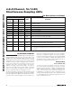
Pin Description (continued)
PIN
MAX11057
(TQFP-EP)
MAX11058
(TQFP-EP)
MAX11059
(TQFP-EP)
NAME FUNCTION
41 41 41 REFIO
External Reference Input/Internal Reference Output. Place a 0.1µF capacitor
from REFIO to AGND.
42 39 37 CH2 Channel 2 Analog Input
44 42 39 CH3 Channel 3 Analog Input
— 44 42 CH4 Channel 4 Analog Input
— 47 44 CH5 Channel 5 Analog Input
— — 47 CH6 Channel 6 Analog Input
— — 50 CH7 Channel 7 Analog Input
61 61 61 WR
Active-Low Write Input. Drive WR low to write to the ADC. Configuration
registers are loaded on the rising edge of WR.
62 62 62 CS
Active-Low Chip-Select Input. Drive CS low when reading from or writing to
the ADC.
63 63 63 RD
Active-Low Read Input. Drive RD low to read from the ADC. Each rising edge
of RD advances the channel output on the data bus.
64 64 64 DB13 14-Bit Parallel Data Bus Digital Out Bit 13
———EP
Exposed Pad. Internally connected to AGND. Connect to a large ground
plane to maximize thermal performance. Not intended as an electrical
connection point.