
Datasheet


MAX105
Dual, 6-Bit, 800Msps ADC with On-Chip,
Wideband Input Amplifier
2 _______________________________________________________________________________________
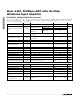
ABSOLUTE MAXIMUM RATINGS
Stresses beyond those listed under “Absolute Maximum Ratings” may cause permanent damage to the device. These are stress ratings only, and functional
operation of the device at these or any other conditions beyond those indicated in the operational sections of the specifications is not implied. Exposure to
absolute maximum rating conditions for extended periods may affect device reliability.
AV
CC
, AV
CC
I, AV
CC
Q and AV
CC
R to AGND............-0.3V to +6V
OV
CC
I and OV
CC
Q to OGND...................................-0.3V to +4V
AGND to OGND ................................................... -0.3V to +0.3V
P0I± to P5I± and A0I± to A5I±
DREADY+, DREADY- to OGNDI .............-0.3V to OV
CC
I+0.3V
P0Q± to P5Q±, A0Q± to A5Q±
DOR+ and DOR- to OGNDQ ................-0.3V to OV
CC
Q+0.3V
REF to AGNDR...........................................-0.3V to AV
CC
R+0.3V
Differential Voltage Between INI+ and INI- ....................-2V, +2V
Differential Voltage Between INQ+ and INQ-.................-2V, +2V
Differential Voltage Between CLK+ and CLK- ...............-2V, +2V
Maximum Current Into Any Pin ...........................................50mA
Continuous Power Dissipation (T
A
= +70°C)
80-Pin TQFP (derate 44mW/°C above +70°C)..................3.5W
Operating Temperature Range
MAX105ECS .....................................................-40°C to +85°C
Junction Temperature......................................................+150°C
Storage Temperature Range .............................-60°C to +150°C
Lead temperature (soldering, 10s) ..................................+300°C
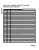
ELECTRICAL CHARACTERISTICS
(AV
CC
= AV
CC
I = AV
CC
Q = AV
CC
R = +5V, OV
CC
I = OV
CC
Q = +3.3V, AGND = AGNDI = AGNDQ = AGNDR = 0, OGNDI = OGNDQ
= 0, f
CLK
= 802.816MHz, C
L
= 1µF to AGND at REF, R
L
= 100Ω ±1% applied to digital LVDS outputs, T
A
= T
MIN
to T
MAX
, unless
otherwise noted. Typical values are at T
A
= +25°C)
PARAMETER SYMBOL CONDITIONS MIN TYP MAX UNITS
DC ACCURACY
Resolution RES 6 Bits
Integral Nonlinearity (Note 1) INL -1 ±0.2 1 LSB
Differential Nonlinearity
(Note 1)
DNL No missing codes guaranteed -1 ±0.25 1 LSB
Offset Voltage V
OS
(Note 2) -1 ±0.25 1 LSB
O ffset M atchi ng Betw een AD C s OM (Note 2) -0.5 ±0.1 0.5 LSB
ANALOG INPUTS (INI+, INI-, INQ+, INQ-)
Input Open-Circuit Voltage V
AOC
2.4 2.5 2.6 V
Input Open-Circuit Voltage
Matching
(V
INI+
- V
IN-
) - (V
INQ+
- V
INQ-
) ±7.5 mV
Common Mode Input Voltage
Range (Note 3)
V
CM
Signal + Offset w.r.t. AGND 1.85 3.05 V
Full-Scale Analog Input
Voltage Range (Note 4)
V
FSR
0.76 0.8 0.84 V
p-p
Input Resistance R
IN
1.7 2 kΩ
Input Capacitance C
IN
1.5 pF
Input Resistance Temperature
Coefficient
TCR
IN
150 ppm/°C
Full-Power Analog Input BW FPBW
-0.5dB
400 MHz
REFERENCE OUTPUT
Reference Output Resistance R
REF
Referenced to AGNDR 5 Ω
Reference Output Voltage √REF I
SOURCE
= 500µA 2.45 2.50 2.55 V