DS87C520/DS83C520 EPROM/ROM High-Speed Microcontrollers www.maxim-ic.
DS87C520/DS83C520 EPROM/ROM High-Speed Microcontrollers ORDERING INFORMATION PART DS87C520-MCL DS87C520-MCL+ DS87C520-QCL DS87C520-QCL+ DS87C520-ECL DS87C520-ECL+ DS87C520-MNL DS87C520-MNL+ DS87C520-QNL DS87C520-QNL+ DS87C520-ENL DS87C520-ENL+ DS87C520-WCL* DS83C520-MCL DS83C520-MCL+ DS83C520-QCL DS83C520-QCL+ DS83C520-ECL DS83C520-ECL+ DS83C520-MNL DS83C520-MNL+ DS83C520-QNL DS83C520-QNL+ DS83C520-ENL DS83C520-ENL+ TEMP RANGE 0˚C to +70˚C 0˚C to +70˚C 0˚C to +70˚C 0˚C to +70˚C 0˚C to +70˚C 0˚C to +70˚C -
DS87C520/DS83C520 EPROM/ROM High-Speed Microcontrollers DESCRIPTION The DS87C520/DS83C520 EPROM/ROM high-speed microcontrollers are fast 8051-compatible microcontrollers. They feature a redesigned processor core without wasted clock and memory cycles. As a result, the devices execute every 8051 instruction between 1.5 and 3 times faster than the original for the same crystal speed. Typical applications will see a speed improvement of 2.5 times using the same code and the same crystal.
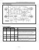
DS87C520/DS83C520 EPROM/ROM High-Speed Microcontrollers Figure 1. Block Diagram DS87C520/ DS83C520 PIN DESCRIPTION DIP 40 20 PIN PLCC 44 1, 22, 23 TQFP 38 16, 17, 39 9 10 4 RST 18 20 14 XTAL2 19 21 15 XTAL1 29 32 26 NAME FUNCTION VCC GND Positive Supply Voltage. +5V Digital Circuit Ground Reset Input. The RST input pin contains a Schmitt voltage input to recognize external active high Reset inputs.
DS87C520/DS83C520 EPROM/ROM High-Speed Microcontrollers PIN DESCRIPTION (continued) DIP PIN PLCC TQFP NAME FUNCTION Address Latch Enable Output. The ALE functions as a clock to latch the external address LSB from the multiplexed address/data bus on Port 0. This signal is commonly connected to the latch enable of an external 373 family transparent latch. ALE has a pulse width of 1.5 XTAL1 cycles and a period of four XTAL1 cycles. ALE is forced high when the DS87C520/DS83C520 are in a reset condition.
DS87C520/DS83C520 EPROM/ROM High-Speed Microcontrollers PIN DESCRIPTION (continued) DIP PIN PLCC TQFP 21 24 18 P2.0 (A8) 22 25 19 P2.1 (A9) 23 26 20 P2.2 (A10) 24 27 21 P2.3 (A11) 25 28 22 P2.4 (A12) 26 29 23 P2.5 (A13) 27 30 24 P2.6 (A14) 28 31 25 P2.7 (A15) 10 11 5 P3.0 11 13 7 P3.1 12 14 8 P3.2 13 15 9 P3.3 14 16 10 P3.4 NAME 15 17 11 P3.5 16 18 12 P3.6 17 19 13 P3.7 31 35 29 EA — 12, 34 6, 28 N.C. FUNCTION Port 2 (A8–15), I/O.
DS87C520/DS83C520 EPROM/ROM High-Speed Microcontrollers COMPATIBILITY The DS87C520/DS83C520 are fully static CMOS 8051-compatible microcontrollers designed for high performance. In most cases, the DS87C520/DS83C520 can drop into an existing socket for the 8xc51 family to improve the operation significantly. While remaining familiar to 8051 family users, the devices have many new features. In general, software written for existing 8051-based systems works without modification on the DS87C520/DS83C520.
DS87C520/DS83C520 EPROM/ROM High-Speed Microcontrollers The relative time of two instructions might be different in the new architecture than it was previously. For example, in the original architecture, the “MOVX A, @DPTR” instruction and the “MOV direct, direct” instruction used two machine cycles or 24 oscillator cycles. Therefore, they required the same amount of time.
DS87C520/DS83C520 EPROM/ROM High-Speed Microcontrollers Table 1. Special Function Register Locations REGISTER P0 SP DPL DPH DPL1 DPH1 DPS PCON TCON TMOD TL0 TL1 TH0 TH1 CKCON PORT1 EXIF SCON0 SBUF0 P2 IE SADDR0 SADDR1 P3 IP SADEN0 SADEN1 SCON1 SBUF1 ROMSIZE PMR STATUS TA T2CON T2MOD RCAP2L RCAP2H TL2 TH2 PSW WDCON ACC EIE B EIP BIT 7 BIT 6 BIT 5 BIT 4 BIT 3 BIT 2 BIT 1 BIT 0 ADDRESS P0.7 P0.6 P0.5 P0.4 P0.3 P0.2 P0.1 P0.
DS87C520/DS83C520 EPROM/ROM High-Speed Microcontrollers MEMORY RESOURCES Like the 8051, the DS87C520/DS83C520 use three memory areas. The total memory configuration of the DS87C520/DS83C520 is 16kB of ROM, 1kB of data SRAM and 256 bytes of scratchpad or direct RAM. The 1kB of data space SRAM is read/write accessible and is memory mapped. This on-chip SRAM is reached by the MOVX instruction. It is not used for executable memory.
DS87C520/DS83C520 EPROM/ROM High-Speed Microcontrollers 16kB internal program space. If software reconfigures the ROMSIZE register to 4kB (0000h–0FFFh) in the current state, the device will immediately jump to external program execution because program code from 4kB to 16kB (1000h–3FFFh) is no longer located on-chip. This could result in code misalignment and execution of an invalid instruction.
DS87C520/DS83C520 EPROM/ROM High-Speed Microcontrollers When disabled, the 1kB memory area is transparent to the system memory map. Any MOVX directed to the space between 0000h and FFFFh goes to the expanded bus on Ports 0 and 2. This also is the default condition. This default allows the DS87C520/DS83C520 to drop into an existing system that uses these addresses for other hardware and still have full compatibility.
DS87C520/DS83C520 EPROM/ROM High-Speed Microcontrollers setting. When desiring maximum speed, software should select a Stretch value of 0. When using very slow RAM or peripherals, select a larger Stretch value. Note that this affects data memory only and the only way to slow program memory (ROM) access is to use a slower crystal. Using a Stretch value between 1 and 7 causes the microcontroller to stretch the read/write strobe and all related timing.
DS87C520/DS83C520 EPROM/ROM High-Speed Microcontrollers POWER MANAGEMENT Along with the standard Idle and power down (Stop) modes of the standard 80C52, the DS87C520/DS83C520 provide a new Power Management Mode. This mode allows the processor to continue functioning, yet to save power compared with full operation. The DS87C520/DS83C520 also feature several enhancements to Stop mode that make it more useful.
DS87C520/DS83C520 EPROM/ROM High-Speed Microcontrollers CRYSTAL-LESS PMM A major component of power consumption in PMM is the crystal amplifier circuit. The DS87C520/DS83C520 allow the user to switch CPU operation to an internal ring oscillator and turn off the crystal amplifier. The CPU would then have a clock source of approximately 2MHz to 4MHz, divided by either 4, 64, or 1024. The ring is not accurate, so software cannot perform precision timing.
DS87C520/DS83C520 EPROM/ROM High-Speed Microcontrollers Switchback To return to a 4-clock rate from PMM, software can simply select the CD1 and CD0 clock control bits to the 4 clocks per cycle state. However, the DS87C520/DS83C520 provide several hardware alternatives for automatic Switchback. If Switchback is enabled, then the device will automatically return to a 4-clock per cycle speed when an interrupt occurs from an enabled, valid external interrupt source.
DS87C520/DS83C520 EPROM/ROM High-Speed Microcontrollers Crystal/Ring Operation The DS87C520/DS83C520 allow software to choose the clock source as an independent selection from the instruction cycle rate. The user can select crystal-based or ring oscillator-based operation under software control. Power-on reset default is the crystal (or external clock) source. The ring may save power depending on the actual crystal speed. To save still more power, software can then disable the crystal amplifier.
DS87C520/DS83C520 EPROM/ROM High-Speed Microcontrollers Table 6. PMM Control and Status Bit Summary BIT LOCATION FUNCTION XT/RG EXIF.3 Control. XT/RG = 1, runs from crystal or external clock; XT/RG = 0, runs from internal ring oscillator. X RGMD EXIF.2 Status. RGMD = 1, CPU clock = ring; RGMD = 0, CPU clock = crystal. 0 CD1, CD0 PMR.7, PMR.6 Control. CD1, 0 = 01, 4 clocks; CS1, 0 = 10, PMM1; CD1, 0 = 11, PMM2. SWB PMR.5 XTOFF PMR.3 PIP HIP LIP XTUP SPTA1 SPRA1 SPTA0 SPRA0 STATUS.
DS87C520/DS83C520 EPROM/ROM High-Speed Microcontrollers Figure 3.
DS87C520/DS83C520 EPROM/ROM High-Speed Microcontrollers IDLE MODE Setting the lsb of the Power Control register (PCON;87h) invokes the Idle mode. Idle will leave internal clocks, serial ports and timers running. Power consumption drops because the CPU is not active. Since clocks are running, the Idle power consumption is a function of crystal frequency. It should be approximately one-half the operational power at a given frequency. The CPU can exit the Idle state with any interrupt or a reset.
DS87C520/DS83C520 EPROM/ROM High-Speed Microcontrollers how the operation would compare when using the ring, and when starting up normally. The default state is to exit Stop mode without using the ring oscillator. The RGSL - Ring Select bit at EXIF.1 (EXIF; 91h) controls this function. When RGSL = 1, the CPU will use the ring oscillator to exit Stop mode quickly. As mentioned above, the processor will automatically switch from the ring to the crystal after a delay of 65,536 crystal clocks. For a 3.
DS87C520/DS83C520 EPROM/ROM High-Speed Microcontrollers PERIPHERAL OVERVIEW The DS87C520/DS83C520 provide several of the most commonly needed peripheral functions in microcomputer-based systems. These new functions include a second serial port, power-fail reset, power-fail interrupt, and a programmable watchdog timer. These are described in the following paragraphs. More details are available in the High-Speed Microcontroller User’s Guide.
DS87C520/DS83C520 EPROM/ROM High-Speed Microcontrollers POWER-FAIL INTERRUPT The voltage reference that sets a precise reset threshold also generates an optional early warning PowerFail Interrupt (PFI). When enabled by software, the processor will vector to program memory address 0033h if VCC drops below VPFW. PFI has the highest priority. The PFI enable is in the Watchdog Control SFR (WDCON–D8h). Setting WDCON.5 to a logic 1 will enable the PFI. Application software can also read the PFI flag at WDCON.4.
DS87C520/DS83C520 EPROM/ROM High-Speed Microcontrollers will set an interrupt flag. Regardless of whether the user enables this interrupt, there are then 512 clocks left until the reset flag is set. Software can enable the interrupt and reset individually. Note that the Watchdog is a free running timer and does not require an enable. There are 5 control bits in special function registers that affect the Watchdog Timer and two status flags that report to the user. WDIF (WDCON.
DS87C520/DS83C520 EPROM/ROM High-Speed Microcontrollers TIMED-ACCESS PROTECTION It is useful to protect certain SFR bits from an accidental write operation. The Timed Access procedure stops an errant CPU from accidentally changing these bits. It requires that the following instructions precede a write of a protected bit. MOV MOV 0C7h, 0C7h, #0Aah #55h Writing an AAh then a 55h to the Timed Access register (location C7h) opens a 3-cycle window for write access.
DS87C520/DS83C520 EPROM/ROM High-Speed Microcontrollers Table 9. EPROM Programming Modes RST PSEN ALE/PROG EA/VPP P2.6 P2.7 P3.3 P3.6 P3.7 Program Code Data H L PL 12.75V L H H H H Verify Code Data H L H H L L L H H Program Encryption Array Address 0-3Fh H L PL 12.75V L H H L H LB1 H L PL 12.75V H H H H H LB2 H L PL 12.75V H H H L L LB3 H L PL 12.75V H L H H L Program Option Register Address FCh H L PL 12.
DS87C520/DS83C520 EPROM/ROM High-Speed Microcontrollers Encryption Array The Encryption Array allows an authorized user to verify EPROM without allowing the true memory to be dumped. During a verify, each byte is Exclusive NORed (XNOR) with a byte in the Encryption Array. This results in a true representation of the EPROM while the Encryption is unprogrammed (FFh). Once the Encryption Array is programmed in a non-FFh state, the verify value will be encrypted.
DS87C520/DS83C520 EPROM/ROM High-Speed Microcontrollers Figure 5. EPROM Programming Configuration ROM-SPECIFIC FEATURES The DS83C520 supports a subset of the EPROM features found on the DS87C520. SECURITY OPTIONS Lock Bits The DS83C520 employs a lock that restricts viewing of the ROM contents. When set, the lock will prevent MOVC instructions in external memory from reading program bytes in internal memory. When locked, the EA pin is sampled and latched on reset.
DS87C520/DS83C520 EPROM/ROM High-Speed Microcontrollers DS83C520 ROM VERIFICATION The DS83C520 memory contents can be verified using a standard EPROM programmer. The memory address to be verified is placed on the pins shown in Figure 5, and the programming control pins are set to the levels shown in Table 9. The data at that location is then asserted on port 0. DS83C520 SIGNATURE The Signature bytes identify the DS83C520 to EPROM programmers. This information is at programming addresses 30h, 31h, and 60h.
DS87C520/DS83C520 EPROM/ROM High-Speed Microcontrollers ABSOLUTE MAXIMUM RATINGS Voltage Range on Any Pin Relative to Ground……………………………………………………….-0.3V to (VCC + 0.5V) Voltage Range on VCC Relative to Ground..………………………………………………………………….-0.3V to +6.0V Operating Temperature Range……………………………………………………………………………….-40°C to +85°C Storage Temperature…………………………………………………………………………………………-55°C to +125°C Soldering Temperature..………………………………………………………..
DS87C520/DS83C520 EPROM/ROM High-Speed Microcontrollers DC ELECTRICAL CHARACTERISTICS (continued) (VCC = 4.5V, TA = -40°C to +85°C.
DS87C520/DS83C520 EPROM/ROM High-Speed Microcontrollers AC ELECTRICAL CHARACTERISTICS (Note 1) PARAMETER Oscillator Frequency External Oscillator External Crystal SYMBOL 1/tCLCL ALE Pulse Width Port 0 Address Valid to ALE Low Address Hold after ALE Low ALE Low to Valid Instruction In ALE Low to PSEN Low tLHLL tAVLL tLLAX1 tLLIV tLLPL PSEN Pulse Width tPLPH tPLIV tPXIX tPXIZ tAVIV1 tAVIV2 tPLAZ PSEN Low to Valid Instruction In Input Instruction Hold after PSEN Input Instruction Float after PSEN Port
DS87C520/DS83C520 EPROM/ROM High-Speed Microcontrollers MOVX CHARACTERISTICS PARAMETER SYMBOL Data Access ALE Pulse Width tLHLL2 Port 0 Address Valid to ALE Low tAVLL2 Address Hold after ALE Low for MOVX Write tLLAX2 RD Pulse Width tRLRH WR Pulse Width tWLWH RD Low to Valid Data In tRLDV Data Hold After Read tRHDX Data Float after Read tRHDZ ALE Low to Valid Data In tLLDV Port 0 Address to Valid Data In tAVDV1 VARIABLE CLOCK MIN MAX 1.5tCLCL-5 2tCLCL-5 0.5tCLCL-5 tCLCL-5 0.
DS87C520/DS83C520 EPROM/ROM High-Speed Microcontrollers MOVX CHARACTERISTICS (continued) M2 0 0 0 0 1 1 1 1 M1 0 0 1 1 0 0 1 1 M0 0 1 0 1 0 1 0 1 MOVX CYCLES 2 machine cycles 3 machine cycles (default) 4 machine cycles 5 machine cycles 6 machine cycles 7 machine cycles 8 machine cycles 9 machine cycles tMCS 0 4 tCLCL 8 tCLCL 12 tCLCL 16 tCLCL 20 tCLCL 24 tCLCL 28 tCLCL EXTERNAL CLOCK CHARACTERISTICS PARAMETER Clock High Time Clock Low Time Clock Rise Time Clock Fall Time SYMBOL MIN tCHCX tCLCX tCLC
DS87C520/DS83C520 EPROM/ROM High-Speed Microcontrollers EXPLANATION OF AC SYMBOLS In an effort to remain compatible with the original 8051 family, the DS87C520 and DS83C520 specify the same parameters as such devices, using the same symbols. For completeness, the following is an explanation of the symbols.
DS87C520/DS83C520 EPROM/ROM High-Speed Microcontrollers 36 of 43
DS87C520/DS83C520 EPROM/ROM High-Speed Microcontrollers EXTERNAL PROGRAM MEMORY READ CYCLE EXTERNAL DATA MEMORY READ CYCLE tAVLL2 37 of 43
DS87C520/DS83C520 EPROM/ROM High-Speed Microcontrollers EXTERNAL DATA MEMORY WRITE CYCLE 2 DATA MEMORY WRITE WITH STRETCH = 1 38 of 43
DS87C520/DS83C520 EPROM/ROM High-Speed Microcontrollers DATA MEMORY WRITE WITH STRETCH = 2 FOUR CYCLE DATA MEMORY WRITE STRETCH VALUE=2 EXTERNAL CLOCK DRIVE 39 of 43
DS87C520/DS83C520 EPROM/ROM High-Speed Microcontrollers SERIAL PORT MODE 0 TIMING SERIAL PORT 0 (SYNCHRONOUS MODE) HIGH SPEED OPERATION SM2=1=>TXD CLOCK=XTAL/4 40 of 43
DS87C520/DS83C520 EPROM/ROM High-Speed Microcontrollers POWER-CYCLE TIMING EPROM PROGRAMMING AND VERIFICATION WAVEFORMS 41 of 43
DS87C520/DS83C520 EPROM/ROM High-Speed Microcontrollers PACKAGE INFORMATION For the latest package outline information, go to www.maxim-ic.com/packages. PACKAGE TYPE PACKAGE CODE DOCUMENT NO.
DS87C520/DS83C520 EPROM/ROM High-Speed Microcontrollers DATA SHEET REVISION SUMMARY REVISION DESCRIPTION 110195 Preliminary release. 022097 1) 2) 3) 4) 5) Update ALE pin description. Add note pertaining to erasure window. Add note pertaining to internal MOVX SRAM. Change Note 10 from RST = 5.5V to RST = VCC. Change serial port mode 0 timing diagram label from tQVXL to tQVXH. 1) 2) 3) 4) 5) 6) Update PMM operating current estimates Added note to clarify IIL specification.