
Datasheet


DS21352/DS21552
104 of 137
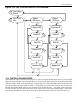
IDENTIFICATION REGISTER
The identification register contains a 32-bit shift register and a 32-bit latched parallel output. This
register is selected during the IDCODE instruction and when the TAP controller is in the Test-Logic-
Reset state. See Table 19-2. Table 19-3 lists the device ID codes for the SCT devices.
Table 19-4 BOUNDARY SCAN CONTROL BITS
BIT PIN SYMBOL TYPE CONTROL BIT DESCRIPTION
2 1 RCHBLK O
2JTMSI
13 8MCLK O
4JTCLKI
5JTRSTI
06 RCL O
7JTDII
8N/C–
9N/C–
10 JTDO O
72 11 BTS I
71 12 LIUC I
70 13 8XCLK O
69 14 TEST I
68 15 NC –
16 RTIP I
17 RRING I
18 RVDD –
19 RVSS –
20 RVSS –
21 MCLK I
22 XTALD O
67 23 NC –
24 RVSS –
66 25 INT O
26 N/C –
27 N/C –
28 N/C –
29 TTIP O
30 TVSS –
31 TVDD –
32 TRING O
65 33 TCHBLK O
64 34 TLCLK O
63 35 TLINK I
62 36 CI I
61 – TSYNC.cntl – 0 = TSYNC an input
1 = TSYNC an output
60 37 TSYNC I/O
Table 19-4 BOUNDARY SCAN CONTROL BITS (cont.)
BIT PIN SYMBOL TYPE CONTROL BIT DESCRIPTION
59 38 TPOSI I
58 39 TNEGI I
57 40 TCLKI I
56 41 TCLKO O
55 42 TNEGO O
54 43 TPOSO O
44 DVDD –