
Datasheet


System Maintenance Interrupt
(SMI) Recovery Stack
An SMI recovery register stack is located in the extend-
ed register bank, locations 4Eh and 4Fh. This register
stack, shown below, can be used by the BIOS to recov-
er from an SMI occurring during an RTC read or write.
The RTC address is latched on the falling edge of the
ALE signal. Each time an RTC address is latched, the
register address stack is pushed. The stack is only four
registers deep, holding the three previous RTC
addresses in addition to the current RTC address being
accessed. Figure 8 illustrates how the BIOS could
recover the RTC address when an SMI occurs.
1) The RTC address is latched.
2) An SMI is generated before an RTC read or write
occurs.
3 RTC address 0Ah is latched and the address from 1
is pushed to the “RTC Address–1” stack location.
This step is necessary to change the bank select bit,
DV0 = 1.
4) RTC address 4Eh is latched and the address from 1
is pushed to location 4Eh, “RTC Address–2” while
0Ah is pushed to the “RTC Address–1” location. The
data in this register, 4Eh, is the RTC address lost due
to the SMI.
DS17285/DS17287/DS17485/DS17487/DS17885/DS17887
Real-Time Clocks
____________________________________________________________________ 27
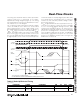
Figure 8. ALE Waveform
RTC ADDRESS
RTC ADDRESS-1
4Eh RTC ADDRESS-2
4Fh RTC ADDRESS-3
SMI Recovery Stack
76543210
DV0 AD6 AD5 AD4 AD3 AD2 AD1 AD0
REGISTER BIT DEFINITION
1
2
3
4
ALE