
Datasheet


I
2
C RTC/Supervisor with Trickle Charger
and 512 Bytes EEPROM
Maxim Integrated 13
DS1388
Control Register (00Ch)
Bit 7: Enable Oscillator (EOSC). When set to logic 0,
the oscillator is started. When set to logic 1, the oscillator
is stopped when the DS1388 switches to battery power.
This setting can be used to conserve battery power
when timekeeping operation is not required. This bit is
cleared (logic 0) when power is first applied. When the
DS1388 is powered by V
CC
, the oscillator is always on
regardless of the status of the EOSC bit. The clock can
be halted whenever the timekeeping functions are not
required, which minimizes V
BAT
current (I
BACKUPDR
).
Bits 6 to 2: These bits read as zero and cannot be
modified.
Bit 1: Watchdog Enable (WDE). When set to logic
one, the watchdog counter is enabled. When set to
logic 0, the watchdog counter is disabled, and the two
registers can be used as NV RAM. This bit is cleared
(logic 0) when power is first applied.
Bit 0: Watchdog Reset (WD/RST). This bit enables the
watchdog alarm output to drive the RST pin. When the
WD/RST bit is set to logic 1, RST pulses low for t
RST
if
WDE = 1 and the watchdog counter reaches zero.
When the WD/RST bit is set to logic 0, the RST pin is
not driven by the watchdog alarm; only the watchdog
flag bit (WF) in the flag register is set to logic 1. This bit
is logic 0 when power is first applied.
Trickle-Charge Register (00Ah)
The simplified schematic of Figure 5 shows the basic
components of the trickle charger. The trickle-charge
select (TCS) bits (bits 4–7) control the selection of the
trickle charger. To prevent accidental enabling, only a
pattern on 1010 enables the trickle charger. All other
patterns disable it. The trickle charger is disabled when
power is first applied. The diode-select (DS) bits (bits 2
and 3) select whether or not a diode is connected
between V
CC
and V
BACKUP
. If DS is 01, no diode is
selected, yet if DS is 10, a diode is selected. The ROUT
bits (bits 0 and 1) select the value of the resistor con-
nected between V
CC
and V
BACKUP
. Table 3 shows the
resistor selected by the resistor select (ROUT) bits and
the diode selected by the diode-select (DS) bits.
Warning: The ROUT value of 250Ω must not be select-
ed whenever V
CC
is greater than 3.63V.
The user determines the diode and resistor selection
according to the maximum current desired for battery
or super cap charging. The maximum charging current
can be calculated as illustrated in the following exam-
ple. Assume that a system power supply of 3.3V is
applied to V
CC
and a super cap is connected to
V
BACKUP
. Also, assume that the trickle charger has
been enabled with a diode and resistor R2 between
V
CC
and V
BACKUP
. The maximum current I
MAX
would
be calculated as follows:
I
MAX
= (3.3V - diode drop) / R2 ≈ (3.3V - 0.7V) / 2kΩ ≈
1.3mA
As the super cap charges, the voltage drop between
V
CC
and V
BACKUP
decreases and therefore the charge
current decreases.
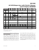
Control Register (00Ch)
BIT 7 BIT 6 BIT 5 BIT 4 BIT 3 BIT 2 BIT 1 BIT 0
EOSC 00000WDEWD/RST
Table 3. Trickle-Charge Register
TCS3
TCS2 TCS1 TCS0
DS1 DS0
ROUT1 ROUT0
FUNCTION
X X X X 0 0 X X Disabled
X X X X 1 1 X X Disabled
X X X X X X 0 0 Disabled
10100101No diode, 250Ω resistor
10101001One diode, 250Ω resistor
10100110No diode, 2kΩ resistor
10101010One diode, 2kΩ resistor
10100111No diode, 4kΩ resistor
10101011One diode, 4kΩ resistor
00000000Initial default value—disabled