
User's Manual


Updated
2008-09-08
File
LEO2 Platform Hardware Manual
Rev.
V1.0
LGE Proprietary
4
MCTR Lab.
1
3. Block description 2
3
3.1 FPGA subsystem 4
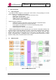
The LEO2-A Platform supports 7 FPGAs (xilinx virtex4 FX140, 1517pin package) for LTE UE 5
modem algorithm. Functionality of each FPGA is 6
- TX FPGA : Transmit block, Viterbi decoder, RF board control 7
- SRCH FPGA : Receiver block 8
- MISO FPGA : Receiver block and MISO 9
- HARQ 0/1 FPGA : Hybrid ARQ block 10
- Turbo Decoder 0/1 FPGA : Decoder block 11
12
Signal connection of FPGAs is 13
- ARM926 bus signal is connected to commonly all FPGAs, except MISO FPGA. 14
- 32 common reserved signals are connected commonly. 15
- 64 test signals of each FPGA are connected to MICTOR probing header. 16
- 4 GPIO LEDs of each FPGAs 17
- Detailed signals are described on block diagram. 18
19
FPGA configure bitstream is stored in platform flash. The maximum configuration bitstream size 20
of virtex4 FX140 is 47,856,896. Bitstream is stored in 2 serial daisy chained memories; capacity is 21
32Mb and 16Mb. Proper binary image should be fused on each platform memories. Xilinx 22
Platform cable connection for image fusing are J12 (TX FPGA), J10 (SRCH FPGA), J7 (MISO 23
FPGA), J3 (HARQ0 FPGA), J4 (HARQ1 FPGA), J6 (Turbo Decoder 0 FPGA) and J1 (Turbo 24
Decoder1 FPGA), which are placed beside of each FPGAs. 25
26
27
3.2 ARM subsystem 28
29
30
Figure 4. ARM processor block 31
32