
Datasheet


28© KEMET Electronics Corporation • KEMET Tower • One East Broward Boulevard T2076_T52X-530 • 4/16/2019
Fort Lauderdale, FL 33301 USA • 954-766-2800 • www.kemet.com
28
KEMET Organic Capacitor (KO-CAP
®
)
T52x/T530 Polymer Electrolytic Capacitors
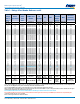
Table 2 – Land Dimensions/Courtyard
T520/T521/T523/T525/T530
KEMET
Metric
Size
Code
Density Level A:
Maximum (Most) Land
Protrusion (mm)
Density Level B:
Median (Nominal) Land
Protrusion (mm)
Density Level C:
Minimum (Least) Land
Protrusion (mm)
Case EIA W L S V1 V2 W L S V1 V2 W L S V1 V2
A 3216–18 1.35 2.20 0.62 6.02 2.80 1.23 1.80 0.82 4.92 2.30 1.13 1.42 0.98 4.06 2.04
B 3528–21 2.35 2.21 0.92 6.32 4.00 2.23 1.80 1.12 5.22 3.50 2.13 1.42 1.28 4.36 3.24
C 6032–28 2.35 2.77 2.37 8.92 4.50 2.23 2.37 2.57 7.82 4.00 2.13 1.99 2.73 6.96 3.74
D 7343–31 2.55 2.77 3.67 10.22 5.60 2.43 2.37 3.87 9.12 5.10 2.33 1.99 4.03 8.26 4.84
H 7360-20 4.25 2.77 3.67 10.22 7.30 4.13 2.37 3.87 9.12 6.80 4.03 1.99 4.03 8.26 6.54
J 7360-15 4.60 3.07 3.07 10.22 7.30 4.48 2.67 3.27 9.12 6.80 4.38 2.29 3.43 8.26 6.54
L 6032-19 2.35 2.77 2.37 8.92 4.50 2.23 2.37 2.57 7.82 4.00 2.13 1.99 2.73 6.96 3.74
M 3528-15 2.35 2.20 0.92 6.32 4.00 2.23 1.80 1.12 5.22 3.50 2.13 1.42 1.28 4.36 3.24
Q 7343-12 2.55 2.77 3.67 10.22 5.60 2.43 2.37 3.87 9.12 5.10 2.33 1.99 4.03 8.26 4.84
T 3528–12 2.35 2.20 0.92 6.32 4.00 2.23 1.80 1.12 5.22 3.50 2.13 1.42 1.28 4.36 3.24
U 6032–15 2.35 2.77 2.37 8.92 4.50 2.23 2.37 2.57 7.82 4.00 2.13 1.99 2.73 6.96 3.74
V 7343–21 2.55 2.77 3.67 10.22 5.60 2.43 2.37 3.87 9.12 5.10 2.33 1.99 4.03 8.26 4.84
W 7343–15 2.55 2.77 3.67 10.22 5.60 2.43 2.37 3.87 9.12 5.10 2.33 1.99 4.03 8.26 4.84
X
1
7343–43 2.55 2.77 3.67 10.22 5.60 2.43 2.37 3.87 9.12 5.10 2.33 1.99 4.03 8.26 4.84
Y
1
7343–40 2.55 2.77 3.67 10.22 5.60 2.43 2.37 3.87 9.12 5.10 2.33 1.99 4.03 8.26 4.84
Density Level A: For low-density product applications. Recommended for wave solder applications and provides a wider process window for reow
solder processes.
Density Level B: For products with a moderate level of component density. Provides a robust solder attachment condition for reow solder processes.
Density Level C: For high component density product applications. Before adapting the minimum land pattern variations the user should perform
qualication testing based on the conditions outlined in IPC standard 7351 (IPC–7351).
¹ Height of these chips may create problems in wave soldering.
2
Land pattern geometry is too small for silkscreen outline.
L
S
W W
L
V1
V2
Grid Placement Courtyard