
Datasheet


IRG4PC40WPbF
2 www.irf.com
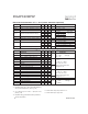
Parameter Min. Typ. Max. Units Conditions
Q
g
Total Gate Charge (turn-on) — 98 147 I
C
= 20A
Q
ge
Gate - Emitter Charge (turn-on) — 12 18 nC V
CC
= 400V See Fig.8
Q
gc
Gate - Collector Charge (turn-on) — 36 54 V
GE
= 15V
t
d(on)
Turn-On Delay Time — 27 —
t
r
Rise Time — 22 — T
J
= 25°C
t
d(off)
Turn-Off Delay Time — 100 150 I
C
= 20A, V
CC
= 480V
t
f
Fall Time — 74 110 V
GE
= 15V, R
G
= 10Ω
E
on
Turn-On Switching Loss — 0.11 — Energy losses include "tail"
E
off
Turn-Off Switching Loss — 0.23 — mJ See Fig. 9,10, 14
E
ts
Total Switching Loss — 0.34 0.45
t
d(on)
Turn-On Delay Time — 25 — T
J
= 150°C,
t
r
Rise Time — 23 — I
C
= 20A, V
CC
= 480V
t
d(off)
Turn-Off Delay Time — 170 — V
GE
= 15V, R
G
= 10Ω
t
f
Fall Time — 124 — Energy losses include "tail"
E
ts
Total Switching Loss — 0.85 — mJ See Fig.10,11, 14
L
E
Internal Emitter Inductance — 13 — nH Measured 5mm from package
C
ies
Input Capacitance — 1900 — V
GE
= 0V
C
oes
Output Capacitance — 140 — pF V
CC
= 30V See Fig. 7
C
res
Reverse Transfer Capacitance — 35 — ƒ = 1.0MHz
Parameter Min. Typ. Max. Units Conditions
V
(BR)CES
Collector-to-Emitter Breakdown Voltage 600 — — V V
GE
= 0V, I
C
= 250µA
V
(BR)ECS
Emitter-to-Collector Breakdown Voltage T 18 — — V V
GE
= 0V, I
C
= 1.0A
∆V
(BR)CES
/∆T
J
Temperature Coeff. of Breakdown Voltage — 0.44 — V/°C V
GE
= 0V, I
C
= 1.0mA
— 2.05 2.5 I
C
= 20A V
GE
= 15V
V
CE(ON)
Collector-to-Emitter Saturation Voltage — 2.36 — I
C
= 40A See Fig.2, 5
— 1.90 — I
C
= 20A , T
J
= 150°C
V
GE(th)
Gate Threshold Voltage 3.0 — 6.0 V
CE
= V
GE
, I
C
= 250µA
∆V
GE(th)
/∆T
J
Temperature Coeff. of Threshold Voltage — 13 — mV/°C V
CE
= V
GE
, I
C
= 250µA
g
fe
Forward Transconductance U 18 28 — S V
CE
= 100 V, I
C
=20A
— — 250 V
GE
= 0V, V
CE
= 600V
— — 2.0 V
GE
= 0V, V
CE
= 10V, T
J
= 25°C
— — 2500 V
GE
= 0V, V
CE
= 600V, T
J
= 150°C
I
GES
Gate-to-Emitter Leakage Current — — ±100 nA V
GE
= ±20V
Electrical Characteristics @ T
J
= 25°C (unless otherwise specified)
I
CES
Zero Gate Voltage Collector Current
V
µA
Switching Characteristics @ T
J
= 25°C (unless otherwise specified)
ns
ns
T Pulse width ≤ 80µs; duty factor ≤ 0.1%.
U Pulse width 5.0µs, single shot.
Notes:
Q Repetitive rating; V
GE
= 20V, pulse width limited by
max. junction temperature. ( See fig. 13b )
R V
CC
= 80%(V
CES
), V
GE
= 20V, L = 10µH, R
G
= 10Ω,
(See fig. 13a)
S Repetitive rating; pulse width limited by maximum
junction temperature.