
User's Manual


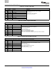


Table Of Contents
- 1 Introduction
- Table of Contents
- 2 Description (continued)
- 3 Physical Characteristics
- 4 ELECTRICAL SPECIFICATIONS
- 5 System Description
- 5.1 Power Supplies
- 5.2 Receiver – Analog Section
- 5.3 Register Descriptions
- 5.4 Direct Commands From MCU to Reader
- 5.4.1 Command Codes
- 5.4.2 Reset
- 5.4.3 Transmission With CRC
- 5.4.4 Transmission Without CRC
- 5.4.5 Delayed Transmission With CRC
- 5.4.6 Delayed Transmission Without CRC
- 5.4.7 Transmission Next Slot
- 5.4.8 Receiver Gain Adjust
- 5.4.9 Test External RF (RSSI at RX input with TX OFF)
- 5.4.10 Test Internal RF (RSSI at RX input with TX ON)
- 5.4.11 Block Receiver
- 5.4.12 Enable Receiver
- 5.5 Reader Communication Interface
- 5.6 Parallel Interface Communication
- 5.7 Serial Interface Communication
- 5.8 External Power Amplifier Application

TRF7960
TRF7961
SLOU186F–AUGUST 2006–REVISED AUGUST 2010
www.ti.com
Table 5-20. RX Special Setting Register (Address 0Ah)
Sets the gains and filters directly
Register default is set to 0x40 at POR = H or EN = L, and at each write to the ISO control register.
Bit Bit Name Function Comments
B7 C212 Bandpass 110 kHz to 570 kHz Appropriate for 212-kHz sub-carrier system
B6 C424 Bandpass 200 kHz to 900 kHz Appropriate for 424-kHz sub-carrier used in ISO15693 and Tag-It
B5 M848 Bandpass 450 kHz to 1.5 MHz Appropriate for Manchester-coded 848-kHz sub-carrier used in ISO14443A
B4 hbt Bandpass 100 kHz to 1.5 MHz Appropriate for highest bit rate (848 kbps) used in high-bit-rate ISO14443
Gain reduced for 7 dB
B3 gd1 01 gain reduction for 5 dB
10 gain reduction for 10 dB Sets the RX gain reduction
B2 gd2
11 gain reduction for 15 dB
B1 agcr AGC activation level change AGC activation level changed from 5 times the digitizing level to 3 times the
digitizing level.
B0 no-lim AGC action is not limited in time AGC action can be done any time during receive process. It is not limited to the
start of receive.
Table 5-21. Regulator and I/O Control (0Bh)
Control the three voltage regulators
Register default is set to 0x87 at POR = H or EN = L
Bit Bit Name Function Comments
B7 auto_reg 0 = setting regulator by option bits Auto system sets VDD_RF to VIN – 250 mV and VDD_A and VDD_X to VIN –
(vrs3_5 and vrs2, vrs1 and vrs0) 250 mV, but not higher than 3.4 V.
1 = automatic setting
B6 en_ext_pa Support for external power Receiver inputs accept externally demodulated sub-carrier, OOK pin becomes
amplifier modulation output for external amplifier.
B5 io_low 1 = enable low peripheral When HIGH, it decreases output resistance of logic outputs. Should be set
communication voltage HIGH when VDD_I/O voltage is below 2.7 V.
B4 Unused Default is LOW.
B3 Unused Default is LOW.
B2 vrs2 Voltage set MSB vrs3_5 = L: VDD_RF, VDD_A, VDD_X range 2.7 V to 3.4 V
B1 vrs1
B0 vrs0 Voltage set LSB
30 System Description Copyright © 2006–2010, Texas Instruments Incorporated
Submit Documentation Feedback
focus.ti.com: TRF7960 TRF7961