
Datasheet


© Copyright 2005-2011 Future Technology Devices International Ltd
8
Document Reference No.: FT_000051
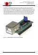
UM232R USB - Serial UART Development Module
Datasheet Version 1.1
Clearance No.: FTDI# 125
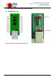
4.2 Signal Descriptions
Pin No.
Name
Type
Description
1
TXD
Output
Transmit Asynchronous Data Output.*
2
DTR#
Output
Data Terminal Ready Control Output / Handshake Signal.*
3
RTS#
Output
Request to Send Control Output / Handshake Signal.*
4
VIO
PWR
+1.8V to +5.25V supply to the UART Interface and CBUS I/O pins (1...3, 5, 6, 9...14,
22, 23).
In USB bus powered designs connect to 3V3 to drive out at 3.3V levels (connect jumper
J1 pins 1 and 2 together), or connect to VCC to drive out at 5V CMOS level (connect
jumper J1 pins 2 and 3 together). This pin can also be supplied with an external 1.8V –
2.8V supply in order to drive out at lower levels. It should be noted that in this case
this supply should originate from the same source as the supply to VCC. This means
that in bus powered designs a regulator which is supplied by the 5V on the USB bus
should be used.
5
RXD
Input
Receiving Asynchronous Data Input.*
6
RI#
Input
Ring Indicator Control Input. When remote wake up is enabled in the internal EEPROM
taking RI# low >20ms can be used to resume the PC USB host controller from
suspend.*
7, 24
GND
PWR
Module Ground Supply Pins
8
DSR#
Input
Data Set Ready Control Input / Handshake Signal.*
9
DCD#
Input
Data Carrier Detect Control Input.
10
CTS#
Input
Clear To Send Control Input / Handshake Signal.*
11
CB4
I/O
Configurable CBUS I/O Pin. Function of this pin is configured in the device internal
EEPROM. Factory Default pin function is SLEEP#. See CBUS Signal Options, Table 4.4.*
12
CB2
I/O
Configurable CBUS I/O Pin. Function of this pin is configured in the device internal
EEPROM. Factory Default pin function is TXDEN. See CBUS Signal Options,Table 4.4.*
13
SLD
GND
USB Cable Shield.
14
USB
Output
5V Power output USB port. For a low power USB bus powered design, up to 100mA can
be sourced from the 5V supply on the USB bus. A maximum of 500mA can be sourced
from the USB bus in a high power USB bus powered design.
15, 21
VCC
PWR or
Output
These two pins are internally connected on the module PCB. To power the module from
the 5V supply on USB bus connects jumper J2 pins 1 and 2 together (this is the module
default configuration). In this case these pins would have the same description as pin
14.
To use the UM232R module in a self powered configuration ensure that jumper J2 pins
1 and 2 are not connected together, and apply an external 4.0V to 5.25V supply to one
of these pins.
17
PU1
Control
Pull up resistor pin connection 2. Connect to pin 20 (RST#) in a self powered
configuration.
16
PU2
Control
Pull up resistor pin connection 1. Connect to pin 14 (USB) in a self powered
configuration.
18
CB3
I/O
Configurable CBUS I/O Pin. Function of this pin is configured in the device internal
EEPROM. Factory Default pin Function is PWREN#. See CBUS Signal Options, Table
4.4.*
19
3V3
Output
3.3V output from integrated L.D.O. regulator. This pin is decoupled to ground on the
module pcb with a 10nF capacitor. The prime purpose of this pin is to provide the
internal 3.3V supply to the USB transceiver cell and the internal 1.5kΩ pull up resistor
on USBDP. Up to 50mA can be drawn from this pin to power external logic if required.
This pin can also be used to supply the FT232RL‟s VCCIO pin by connecting this pin to
pin 4 (VIO), or by connecting together pins 1 and 2 on jumper J1.