
Datasheet


LMV321/LMV358/LMV324 DATA SHEET
REV. 1D. Feb. 2012
7
Application Information
General Description
voltage-feedback amplifiers that are pin-for-pin compatible
and drop in replacements with other industry standard
LMV321, LMV358, and LMV324 amplifiers. The LMV3XX
family is fabricated on a CMOS process, features a rail-to-rail
output, and is unity gain stable.
The typical non-inverting circuit schematic is shown in Figure
1.
Figure 1: Typical Non-inverting configuration
Power Dissipation
The maximum internal power dissipation allowed is directly
related to the maximum junction temperature. If the maximum
junction temperature exceeds 150°C, some performance
degradation will occur. If the maximum junction temperature
exceeds 175°C for an extended time, device failure may occur.
Driving Capacitive Loads
The Frequency Response vs C
L
plot on page 4, illustrates the
response of the LMV3XX family. A small series resistance (R
s
)
at the output of the amplifier, illustrated in Figure 2, will improve
stability and settling performance. R
s
values in the Frequency
Response vs C
L
plot were chosen to achieve maximum band-
width with less than 1dB of peaking. For maximum flatness,
use a larger R
s
. As the plot indicates, the LMV3XX family
can easily drive a 200pF capacitive load without a series
resistance. For comparison, the plot also shows the LMV321
driving a 200pF load with a 225Ω series resistance.
Driving a capacitive load introduces phase-lag into the output
signal, which reduces phase margin in the amplifier. The
unity gain follower is the most sensitive configuration. In a
unity gain follower configuration, the LMV3XX family
requires a 450Ω series resistor to drive a 200pF load. The
response is illustrated in Figure 3.
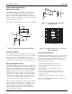
Figure 2: Typical Topology for driving a
capacitive load
Figure 3: Frequency Response vs C
L
for unity
gain configuration
Layout Considerations
General layout and supply bypassing play major roles in high
frequency performance. Fairchild has evaluation boards to
use as a guide for high frequency layout and as aid in device
testing and characterization. Follow the steps below as a
basis for high frequency layout:
• Include 6.8µF and 0.01µF ceramic capacitors
• Place the 6.8µF capacitor within 0.75 inches of
the power pin
• Place the 0.01µF capacitor within 0.1 inches of
the power pin
• Remove the ground plane under and around the part,
especially near the input and output pins to reduce
parasitic capacitance
• Minimize all trace lengths to reduce series inductances
Refer to the evaluation board layouts shown in Figure 5 on
page 8 for more information.
+
-
LMV3XX
R
f
0.01µF
6.8µF
Out
+In
+V
s
+
R
g
+
-
10kΩ
10kΩ
R
s
C
L
2kΩ
LMV3XX
Magnitude (dB)
Frequency (MHz)
0.01 0.1 1 10
-9
-8
-7
-6
-5
-4
-3
-2
-1
0
1
2
3
C
L
= 50pF
R
s
= 0
C
L
= 100pF
R
s
= 400Ω
C
L
= 200pF
R
s
= 450Ω
The LMV3XX family are dual supply, general purpose,