
Datasheet


FPF2300/02/03 — Dual-Output Current Limit Switch
© 2009 Fairchild Semiconductor Corporation www.fairchildsemi.com
FPF2300/02/03 • Rev. 1.1.3 3
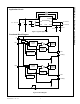
Pin Configuration
Figure 5. Pin Configurations
Pin Description
Pin # Name Function
1 GND Ground
2 IN Supply Input: Input to the power switch and the supply voltage for the IC.
3 ONA ON / OFF control input of power switch A. Active LOW
4 ONB ON / OFF control input of power switch B. Active LOW
5FLAGB(B)
Fault Output B, Active LO, open drain output which indicates an over supply, UVLO
and thermal shutdown.
6 OUTB Switch Output: Output of the power switch B
7 OUTA Switch Output: Output of the power switch A
8FLAGB(A)
Fault Output A, Active LO, open drain output which indicates an over supply, UVLO
and thermal shutdown.
9(MLP) Thermal Pad
IC Substrate, which can be connected to GND for better thermal performance. Do not
connect to other pins.
SO8
1
GND
2
3
4
8
7
6
5
IN
ONA
ONB
FLAGB(A)
OUTA
OUTB
FLAGB(B)
GND
IN
ONAOUTB
FLAGB(A)
MLP 3X3mm 8-Lead Bottom View
8
7
63
2
1
OUTA
FLAGB(B)
5
ONB
4
9