
Operator's Manual


CIRCUIT DESCRIPTION
4-5
September 2001
Part No. 001-5100-001
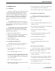
Figure 4-2 RF Board Block Diagram
5. When the voltage gets really low, the 5 volt DC/DC
converter automatically shuts down.
6. The 5-volt analog and switched RF B+ sources turn
off.
4.3 RF BOARD CIRCUIT DESCRIPTION
4.3.1 FREQUENCY GENERATION UNIT
The Frequency Generation Unit (FGU) consists
of these three major sections: (1) high stability refer-
ence oscillator, (2) fractional-N synthesizer, and (3)
VCO buffer. A 5-volt regulator supplies power to the
FGU. The regulator output voltage is filtered and then
distributed to the transmit and receive VCOs and the
VCO buffer IC. The mixer LO injection signal and
transmit frequency are generated by the receive VCO
and transmit VCO, respectively. The receive VCO
uses an external active device, and the transmit VCO
active device is a transistor inside the VCO buffer.
The receive VCO is a Colpitts-type oscillator.
The receive VCO signal is received by the VCO buffer
where it is amplified by a buffer inside the IC. The
amplified signal is routed through a low-pass filter and
injected as the first LO signal into the mixer. In the
VCO buffer, the receive VCO signal is also routed to
an internal prescaler buffer. The buffered output is
applied to a low-pass filter. After filtering, the signal is
routed to a prescaler divider in the synthesizer.
The divide ratios for the prescaler circuits are
determined from information stored in an EEPROM.
The microprocessor extracts data for the division ratio
as determined by the position of the channel-select
switch and routes the signal to a comparator in the
synthesizer. A 16.8 MHz reference oscillator applies
the 16.8 MHz signal to the synthesizer. The oscillator
signal is divided into one of three pre-determined
frequencies. A time-based algorithm is used to
generate the fractional-N ratio.
If the two frequencies in the synthesizer’s
comparator differ, an error voltage is produced. The
phase detector error voltage is applied to the loop
filter. The filtered voltage alters the VCO frequency
until the correct frequency is synthesized.
In the transmit mode, the modulation of the
carrier is achieved by using a two-port modulation
technique. The modulation for low frequency tones,
such as CTCSS and DCS, is achieved by injecting the
tones into the A/D section of the fractional-N divider,
generating the required deviation. Modulation of the
high frequency audio signals is achieved by modu-
lating the varactor through a frequency compensation
network.
RF BOARD