
User`s manual


44
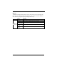
Phienix – AwardBIOS CMOS Setup Utility
DRAM Clock/ Drive Control
Current FSB Fre
q
uenc
y
I
tem Hel
p
Current DRAM Frequency
Menu Level
"
DRAM Clock By SPD
DRAM Timing Manual
DRAM CAS Latency 2.5
Bank Interleave Disabled
Precharge to Active (Trp) 3T
Active to Precharge (Tras) 6T
Active to CMD (Trcd) 3T
DRAM Burst Length 4
DRAM Queue Depth 4 level
DRAM Command Rate 2T Command
↑
↓
→
←
: Move Enter: Select + / - /PU / PD: value F10: save ESC: Exit F1: General Help
F5 : Previous Values F6:Fail-Safe Defaults F7: Optimized Defaults
DRAM Control
Values Meaning
By SPD
100 MHz
If your DIMM modules are PC-100 compliant, select this
setting.
DRAM Clock
133 MHz
Only when your DIMM modules are PC-133 compliant can you
use this setting. In case of instability always select 100MHz.
Manual
DRAM
Timing
By SPD
2
DRAM CAS
Latency
2.5
Disabled This is the safest setting (default).
2 bank This setting is faster than disabled.
Bank
Interleave
4 bank This is fastest setting.
4
DRAM Burst
Length
8
2T level
3T level
DRAM
Queue Depth
4T level
DRAM
Command
2T
Command