
Datasheet


CONTROL
LOGIC
SUCCESSIVE
APPROXIMATION
ADC
SCLK
CS
SDATA
V
IN
T/H
ADCS7476
ADCS7477
ACDS7478
Copyright © 2016, Texas Instruments Incorporated
16
ADCS7476
,
ADCS7477
,
ADCS7478
SNAS192G –APRIL 2003–REVISED MAY 2016
www.ti.com
Product Folder Links: ADCS7476 ADCS7477 ADCS7478
Submit Documentation Feedback Copyright © 2003–2016, Texas Instruments Incorporated
7 Detailed Description
7.1 Overview
The ADCS747x devices are successive-approximation analog-to-digital converters designed around a charge-
redistribution digital-to-analog converter. Simplified schematics of the ADCS747x in both track and hold operation
are shown in Figure 25 and Figure 26. In Figure 26, the device is in track mode where the switch SW1 connects
the sampling capacitor to the input, and SW2 balances the comparator inputs. The device is in this state until CS
is brought low, at which point the device moves to hold mode.
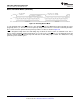
7.2 Functional Block Diagram
7.3 Feature Description
Serial interface timing diagrams for the ADCS747x are shown in Figure 2, Figure 3, and Figure 4. CS is chip
select, which initiates conversions and frames the serial data transfers. SCLK (serial clock) controls both the
conversion process and the timing of serial data. SDATA is the serial data out pin, where a conversion result is
found.
Basic operation of the ADCS747x begins with CS going low, which initiates a conversion process and data
transfer. Subsequent rising and falling edges of SCLK will be labeled with reference to the falling edge of CS; for
example, the third falling edge of SCLK shall refer to the third falling edge of SCLK after CS goes low.
At the fall of CS, the SDATA pin comes out of TRI-STATE, and the converter moves from track mode to hold
mode. The input signal is sampled and held for conversion at the falling edge of CS. The converter moves from
hold mode to track mode on the 13th rising edge of SCLK (see Figure 2, Figure 3, or Figure 4). The SDATA pin
is placed back into TRI-STATE after the 16th falling edge of SCLK, or at the rising edge of CS, whichever occurs
first. After a conversion is completed, the quiet time t
QUIET
must be satisfied before bringing CS low again to
begin another conversion.
Sixteen SCLK cycles are required to read a complete sample from the ADCS747x. The sample bits (including
any leading or trailing zeroes) are clocked out on falling edges of SCLK, and are intended to be clocked in by a
receiver on subsequent falling edges of SCLK. ADCS747x produces four leading zeroes on SDATA, followed by
twelve, ten, or eight data bits (the most significant first). After the data bits, the ADCS7477 clocks out two trailing
zeros, and the ADCS7478 clocks out four trailing zeros. The ADCS7476 does not clock out any trailing zeros; the
least significant data bit is valid on the 16th falling edge of SCLK.
Depending upon the application, the first edge on SCLK after CS goes low may be either a falling edge or a
rising edge. If the first SCLK edge after CS goes low is a rising edge, all four leading zeroes are valid on the first
four falling edges of SCLK. If instead the first SCLK edge after CS goes low is a falling edge, the first leading
zero may not be set up in time for a microprocessor or DSP to read it correctly. The remaining data bits are still
clocked out on the falling edges of SCLK.