
User Guide


III. IMAGE PROCESSING
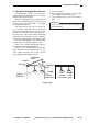
A. Outline
The image processing system converts the optical image projected on the CCD into electrical signals
(image signals) for correction and processing.
The correction/processing functions are by the following PCBs, and the results of correction/process-
ing are forwarded to the PCBs that follow them:
Figure 3-301
Analog processor
PCB
Image processor PCB
Laser driver
PCB
CCD
A-D
conversion
circuit
Shading
correction
circuit
Image
processing
circuit
Laser
driver
circuit
G3 FAX
Board/NCU
D/A
conversion
Binary
processing
Binary
processing
for fax
Reproduction
ratio
processing
CORE/IP
Board
Video signal
switching circuit
Command conversion
circuit
Protocol controller PCB
Printer
Board
Network I/F
Board
3–29
COPYRIGHT © 1996 CANON INC. CANON GP215/200 REV.0 JULY 1996 PRINTED IN JAPAN (IMPRIME AU JAPON)
3. OPERATIONS AND TIMING